Äîêóìåíòàöèÿ è îïèñàíèÿ www.docs.chipfind.ru

8-BIT SINGLE-CHIP MICROCONTROLLERS
GMS77C1000
GMS77C1001
User's Manual
(Ver. 1.1)

Version 1.1
Published by
MCU Application Team
©
©
©
©
2001 Hynix Semiconductor All right reserved.
Additional information of this manual may be served by Hynix Semiconductor offices in Korea or Distributors and Representatives listed
at address directory.
Hynix Semiconductor reserves the right to make changes to any information here in at any time without notice.
The information, diagrams and other data in this manual are correct and reliable; however, Hynix Semiconductor is in no way responsible
for any violations of patents or other rights of the third party generated by the use of this manual.

GMS77C1000/GMS77C1001
July. 2001 Ver 1.1
Contents of Table
OVERVIEW . . . . . . . . . . . . . . . . . . . . . . . . . 1
Description . . . . . . . . . . . . . . . . . . . . . . . . . . . . 1
Features . . . . . . . . . . . . . . . . . . . . . . . . . . . . . . 1
BLOCK DIAGRAM . . . . . . . . . . . . . . . . . . . 2
PIN ASSIGNMENT . . . . . . . . . . . . . . . . . . . 3
PACKAGE DIAGRAM . . . . . . . . . . . . . . . . . 4
PIN FUNCTION . . . . . . . . . . . . . . . . . . . . . . 6
PORT STRUCTURES . . . . . . . . . . . . . . . . . 7
ELECTRICAL CHARACTERISTICS . . . . . . 9
Absolute Maximum Ratings . . . . . . . . . . . . . . . 9
Recommended Operating Conditions . . . . . . . 9
DC Characteristics (1) . . . . . . . . . . . . . . . . . . 10
DC Electrical Characteristics (2) . . . . . . . . . . 11
AC Electrical Characteristics (1) . . . . . . . . . . 12
AC Electrical Characteristics (2) . . . . . . . . . . 13
Typical Characteristics . . . . . . . . . . . . . . . . . . 14
ARCHITECTURE . . . . . . . . . . . . . . . . . . . 17
CPU Architecture . . . . . . . . . . . . . . . . . . . . . . 17
MEMORY . . . . . . . . . . . . . . . . . . . . . . . . . . 18
Program Memory . . . . . . . . . . . . . . . . . . . . . . 18
Data Memory . . . . . . . . . . . . . . . . . . . . . . . . . 18
Special Function Registers . . . . . . . . . . . . . . 19
I/O PORTS . . . . . . . . . . . . . . . . . . . . . . . . . 23
Port RA . . . . . . . . . . . . . . . . . . . . . . . . . . . . . 23
Port RB . . . . . . . . . . . . . . . . . . . . . . . . . . . . . . 23
I/O Interfacing . . . . . . . . . . . . . . . . . . . . . . . . . 23
I/O Successive Operations . . . . . . . . . . . . . . . 23
TIMER0 MODULE AND TMR0 REGISTER 25
Timer Mode . . . . . . . . . . . . . . . . . . . . . . . . . . 26
Counter Mode . . . . . . . . . . . . . . . . . . . . . . . . 26
Using Timer0 with an External Clock . . . . . . . 27
Prescaler . . . . . . . . . . . . . . . . . . . . . . . . . . . . 27
CONFIGURATION AREA . . . . . . . . . . . . . 29
OSCILLATOR CIRCUITS . . . . . . . . . . . . . 30
XT, HF or LF Mode . . . . . . . . . . . . . . . . . . . . 30
RC Oscillation Mode . . . . . . . . . . . . . . . . . . . 30
RESET . . . . . . . . . . . . . . . . . . . . . . . . . . . . 32
Power-On Reset (POR) . . . . . . . . . . . . . . . . . 33
Internal Reset Timer (IRT) . . . . . . . . . . . . . . . 35
WATCHDOG TIMER (WDT) . . . . . . . . . . . 36
WDT Period . . . . . . . . . . . . . . . . . . . . . . . . . . 36
WDT Programming Considerations . . . . . . . . 36
Power-Down Mode (SLEEP) . . . . . . . . . . 37
SLEEP . . . . . . . . . . . . . . . . . . . . . . . . . . . . . . 37
Wake-up From SLEEP . . . . . . . . . . . . . . . . . . 38
Minimizing Current Consumption . . . . . . . . . . 38
TIME-OUT SEQUENCE AND POWER DOWN
STATUS BITS (TO/PD) . . . . . . . . . . . . . 40
POWER FAIL DETECTION PROCESSOR 41
GMS77C1000/GMS77C1001
July. 2001 Ver. 1.1
1
GMS77C1000 / GMS77C1001
CMOS SINGLE-CHIP 8-BIT MICROCONTROLLER
1. OVERVIEW
1.1 Description
The GMS77C1000 and GMS77C1001 are an advanced CMOS 8-bit microcontroller with 0.5K/1K words(12-bit) of
EPROM. The Hynix Semiconductor GMS77C1000 and GMS77C1001 are a powerful microcontroller which provides a high
flexibility and cost effective solution to many small applications. The GMS77C1000 and GMS77C1001 provide the follow-
ing standard features: 0.5K/1K words of EPROM, 25 bytes of RAM, 8-bit timer/counter, power-on reset, on-chip oscillator
and clock circuitry. In addition, the GMS77C1000 and GMS77C1001 supports power saving modes to reduce power con-
sumption.
1.2 Features
· High-Performance RISC CPU:
- 12-bit wide instructions and 8-bit wide data path
- 33 single word instructions
- 0.5K/1K words on-chip program memory
- 25 bytes on-chip data memory
- Minimum instruction execution time
200ns @20MHz
- Operating speed: DC - 20 MHz clock input
- Seven special function hardware registers
- Two-level hardware stack
· Peripheral Features:
- Twelve programmable I/O lines
- One 8-bit timer/counter with 8-bit programmable
prescaler
- Power-On Reset (POR)
- Power Fail Detector : noise immunity circuit
2 level detect ( 3V, 2.5V )
- Internal Reset Timer (IRT)
- Watchdog Timer (WDT) with on-chip RC oscilla-
tor
- Programmable code-protection
- Power saving SLEEP mode
- Selectable oscillator options: Configuration word
RC: Low-cost RC oscillator (200KHz~4MHz)
XT: Standard crystal/resonator (455KHz~4MHz)
HF: High-speed crystal/resonator (4~20MHz)
LF: Power saving, low-frequency crystal/resonator
(32~200KHz)
· CMOS Technology:
- Low-power, high-speed CMOS EPROM technol-
ogy
- Fully static design
- Wide-operating
range:
2.5V to 5.5V @ RC, XT, LF
4.5V to 5.5V @ HF
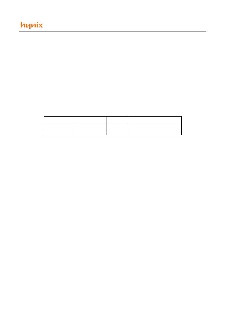
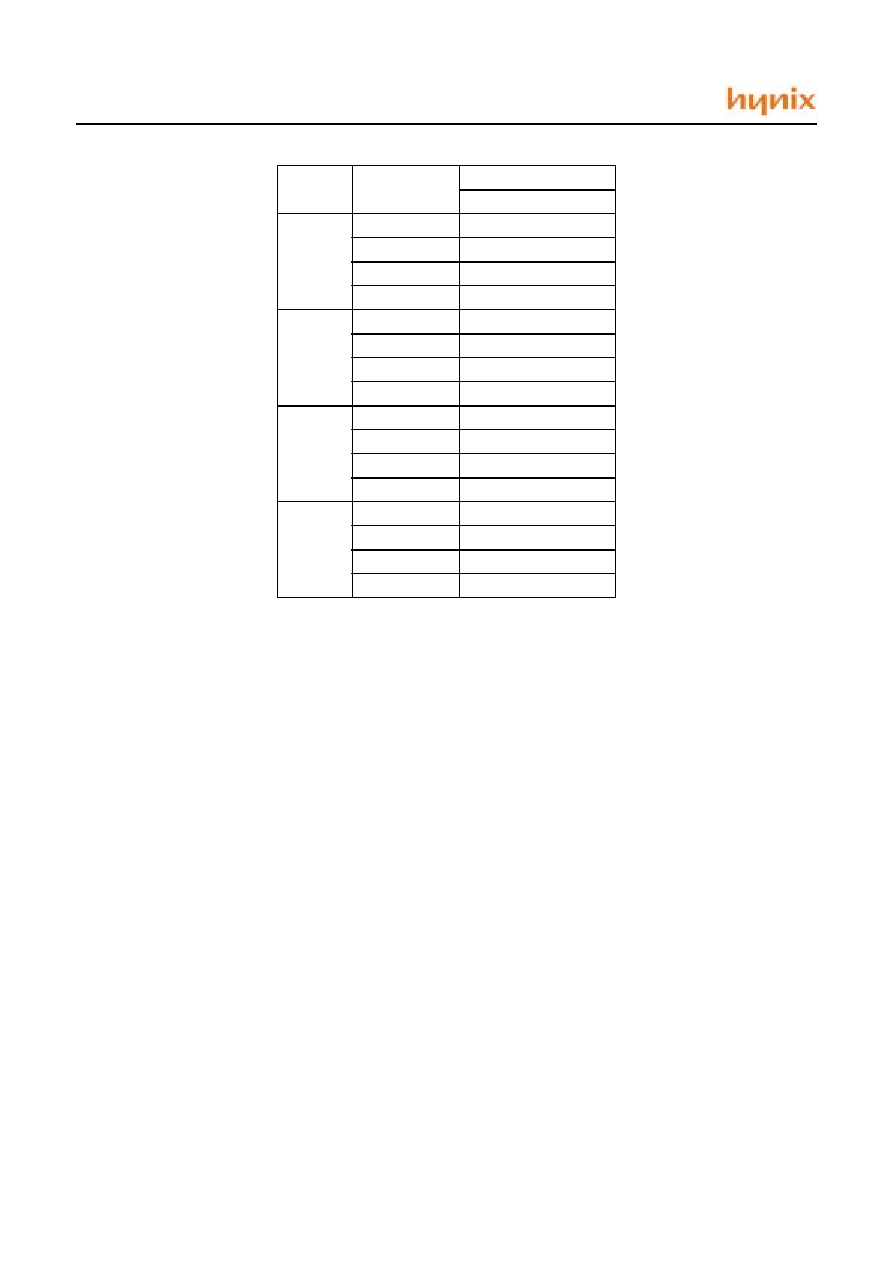
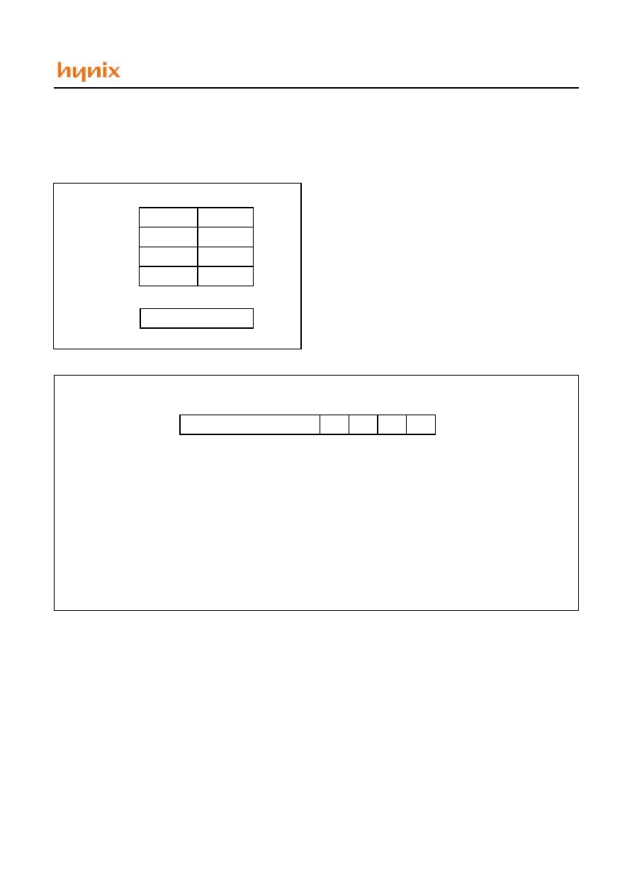
Device name
ROM Size
RAM Size
Package
GMS77C1000
0.5K words(12-bit)
25 bytes
18 PDIP, SOP or 20 SSOP
GMS77C1001
1K words(12-bit)
25 bytes
18 PDIP, SOP or 20 SSOP
GMS77C1000/GMS77C1001
2
July. 2001 Ver. 1.1
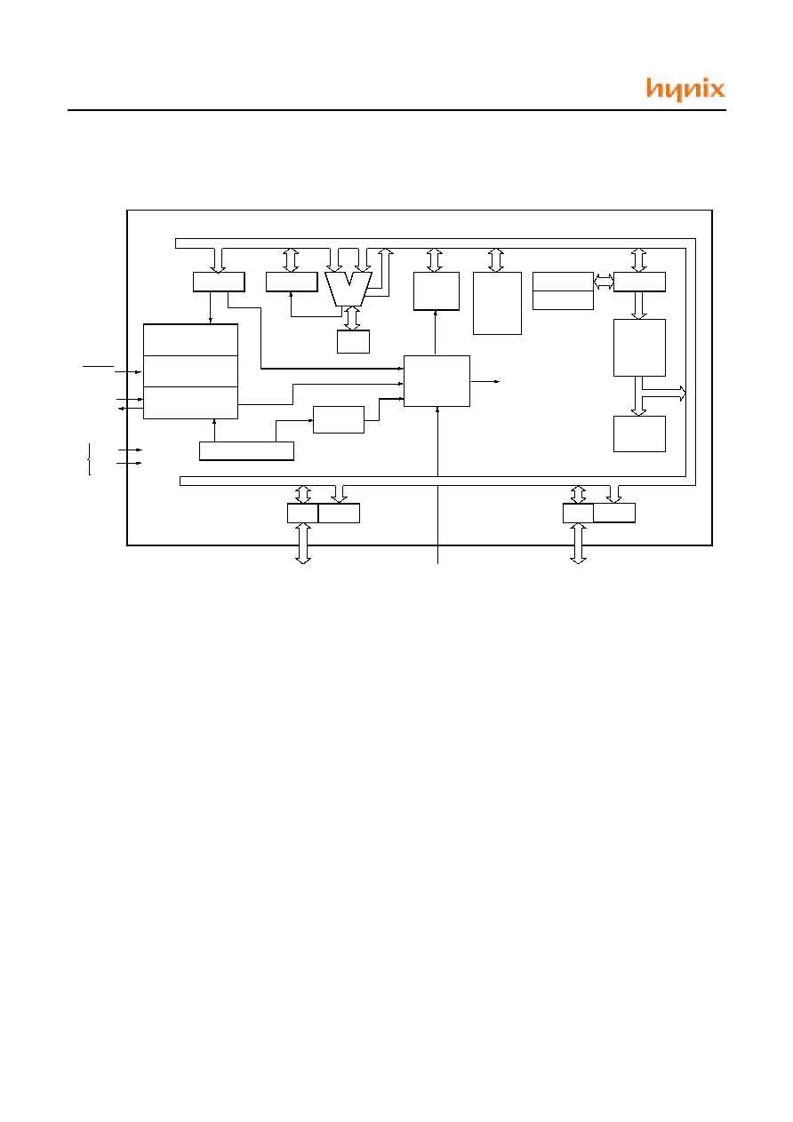
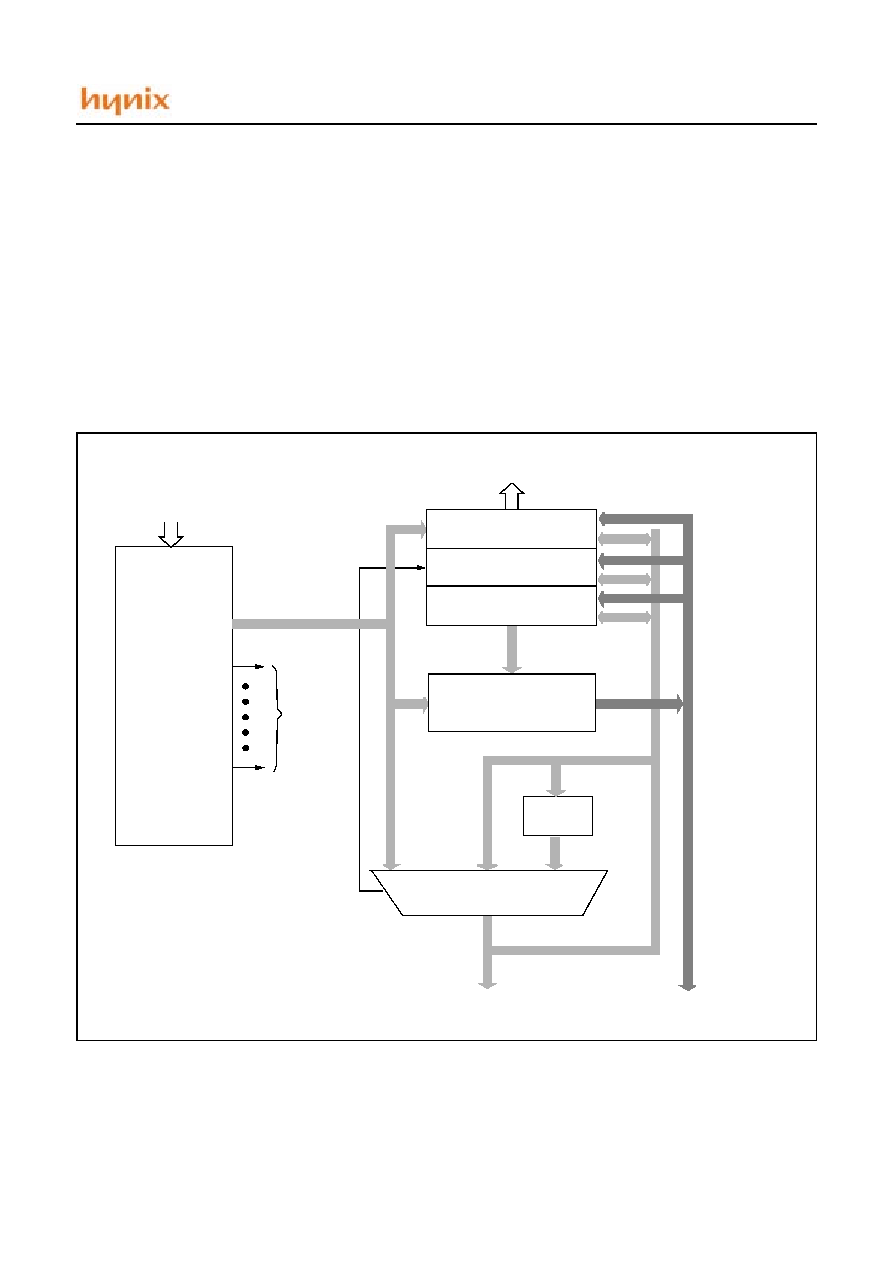
2. BLOCK DIAGRAM
W
STACK 1
Data
Memory
8-bit
Counter
Timer/
Program
Memory
PC
WDT/
Prescaler
Watch-dog
Timer
Instruction
RA
RB
STATUS
System controller
Clock Generator
RESET
Xin
Xout
RA0
RA1
RA2
RA3
RB0
RB1
RB2
RB3
RB4
V
DD
V
SS
Power
Supply
Decoder
RB5
RB6
RB7
EC0
WDT time out
ALU
STACK 2
OPTION
TMR0
Power Fail Detector
Timing Control
Configuration Word
TRISA
TRISB
GMS77C1000/GMS77C1001
July. 2001 Ver. 1.1
3
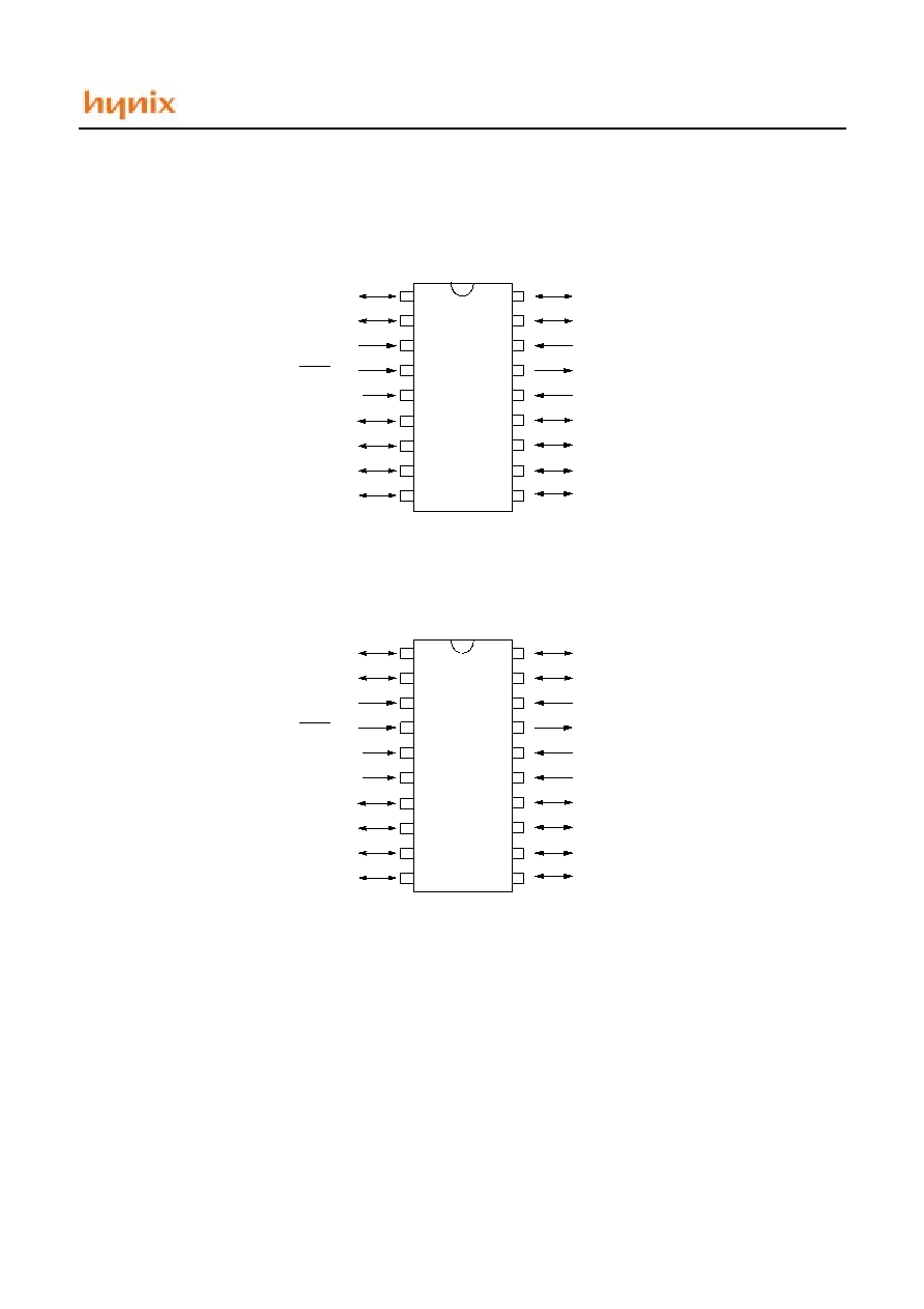
3. PIN ASSIGNMENT
V
SS
RA1
RA0
Xin
Xout
V
DD
RB7
RB6
RB5
RA2
RA3
EC0
RESET/V
PP
V
SS
RB0
RB1
RB2
RB3
18 PDIP or SOP
1
2
3
4
5
6
7
8
9
18
17
16
15
14
13
12
11
10
RB4
RA1
RA0
Xin
Xout
V
DD
RB7
RB6
RB5
RA2
RA3
EC0
RESET/V
PP
V
SS
RB0
RB1
RB2
RB3
20 SSOP
RB4
V
DD
5
1
2
3
4
6
7
8
9
10
20
19
14
18
17
15
13
12
11
16
GMS77C1000/GMS77C1001
4
July. 2001 Ver. 1.1
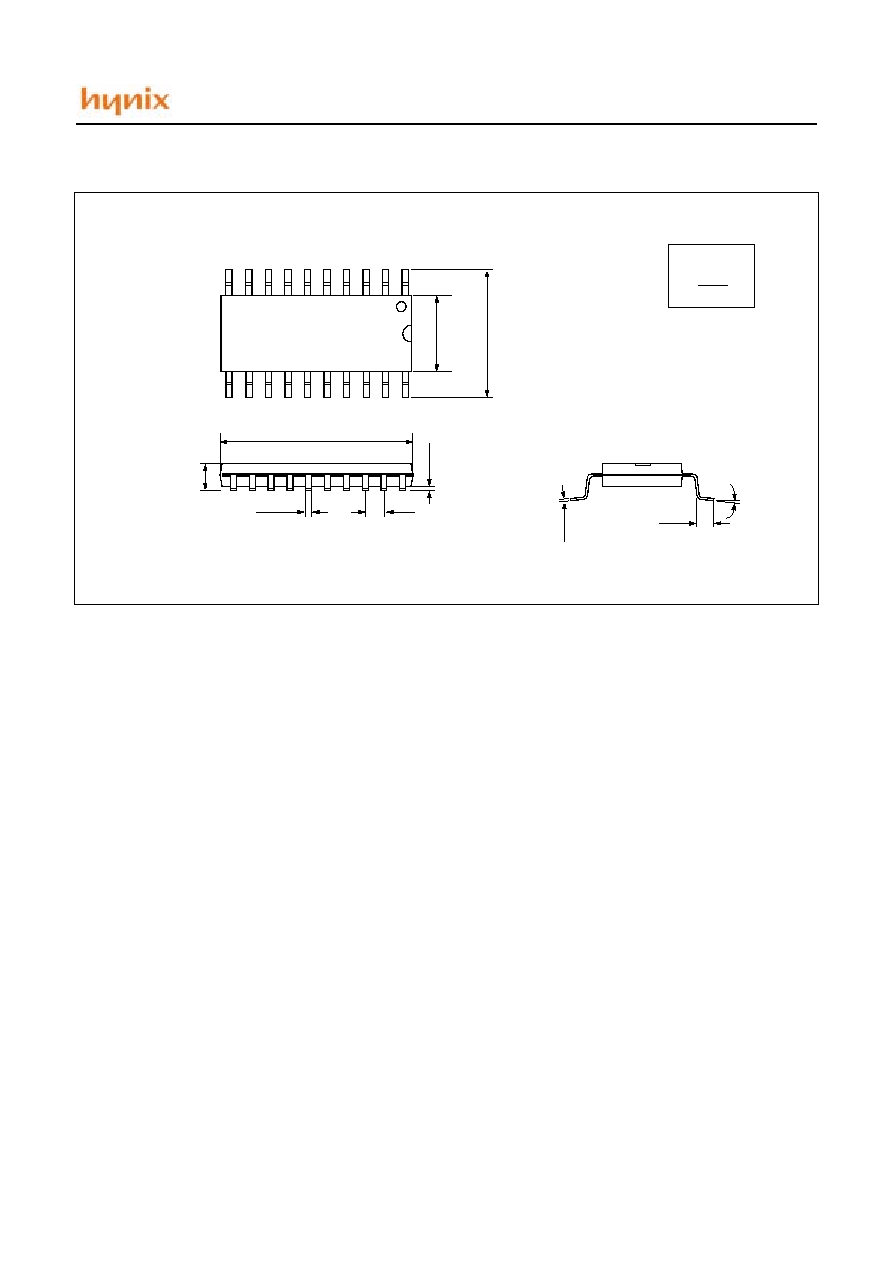
4. PACKAGE DIAGRAM
0.925
0.0 15
0.045
TYP 0.10
TYP 0.300
0.270
0.01
5
0 ~ 15°
MA
X 0.
180
MIN 0.020
0.120
0.292
0.
4
0
0
0.461
0.
1
0
4
0.014
TYP 0.050
0.005
0.
0091
0 ~ 8°
0.024
18 PDIP
18 SOP
unit: inch
MAX
MIN
0.895
0.022
0.140
0.065
0.00
8
0.245
0.410
0.299
0.451
0.
0
9
7
0.029
0.040
0.
0125
0.01
15
GMS77C1000/GMS77C1001
July. 2001 Ver. 1.1
5
0.205
0.
3
0
1
0.289
0.
0
7
8
0.010
TYP 0.0256
0.002
0.
004
0 ~ 8°
0.025
20 SSOP
unit: inch
MAX
MIN
0.31
1
0.212
0.278
0.
0
6
8
0.015
0.037
0.
008
0.008
GMS77C1000/GMS77C1001
6
July. 2001 Ver. 1.1
5. PIN FUNCTION
V
DD
: Supply voltage.
V
SS
: Circuit ground.
RESET: Reset the MCU.
X
IN
: Input to the inverting oscillator amplifier and input to
the internal main clock operating circuit.
X
OUT
: Output from the inverting oscillator amplifier.
RA0~RA3: RA is an 4-bit, CMOS, bidirectional I/O port.
RA pins can be used as outputs or inputs according to "0"
or "1" written the their Port Direction Register(TRISA).
RB0~RB7: RB is a 8-bit, CMOS, bidirectional I/O port.
RB pins can be used as outputs or inputs according to "0"
or "1" written the their Port Direction Register(TRISB).
EC0: EC0 is an external clock input to Timer0. It should
be tied to V
SS
or V
DD
, if not in use, to reduce current con-
sumption.
Legend : I =input, O = output, I/O = input/output, P = power, - = Not used, TTL = TTL input, ST = Schmitt Trigger input
PIN NAME
DIP, SOP
Pin No.
SSOP
Pin No.
In/Out
Input
Levels
Function
V
DD
14
15,16
P
-
Supply voltage
V
SS
5
5,6
P
-
Circuit ground
RESET
4
4
I
ST
Reset signal input/programming voltage input. This pin is an active low
reset to the device. Voltage on the RESET pin must not exceed V
DD
to
avoid unintended entering of programming mode.
X
IN
16
18
I
ST
Oscillator crystal input/external clock source input
X
OUT
15
17
O
-
Oscillator crystal output. Connects to crystal or resonator in crystal oscilla-
tor mode. In RC mode, X
OUT
pin outputs CLKOUT which has 1/4 the fre-
quency of X
IN
, and denotes the instruction cycle rate.
RA0
17
19
I/O
TTL
4-bit bi-directional I/O ports
RA1
18
20
I/O
TTL
RA2
1
1
I/O
TTL
RA3
2
2
I/O
TTL
RB0
6
7
I/O
TTL
8-bit bi-directional I/O ports
RB1
7
8
I/O
TTL
RB2
8
9
I/O
TTL
RB3
9
10
I/O
TTL
RB4
10
11
I/O
TTL
RB5
11
12
I/O
TTL
RB6
12
13
I/O
TTL
RB7
13
14
I/O
TTL
EC0
3
3
I
ST
Clock input to Timer0. Must be tied to V
DD
or V
SS
, if not in use, to reduce
current consumption.
TABLE 5-1 PINOUT DESCRIPTION
GMS77C1000/GMS77C1001
July. 2001 Ver. 1.1
7
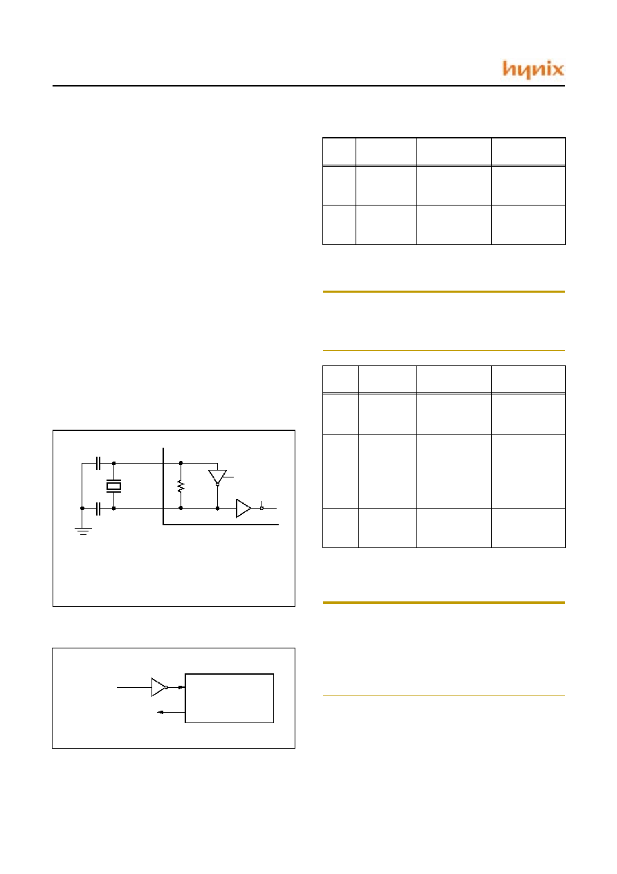
6. PORT STRUCTURES
· RESET
· Xin, Xout
V
SS
Internal RESET
V
SS
Xout
Xin
Amplifier varies with
To Internal Clock
V
DD
V
SS
Xout
Xin
V
DD
÷
÷
÷
÷
4
( XT, HF, LF Mode )
EN ( XT, HF, LF )
R
F
EN ( RC )
( RC Mode )
the oscillation mode
Internal
Capacitance ( appx. 6pF )
To Internal Clock
GMS77C1000/GMS77C1001
8
July. 2001 Ver. 1.1
· RA0~3/RB0~7
· EC0
Data Bus
Data Bus
Data Bus
Data Reg.
Direction Reg.
Read
V
DD
V
SS
V
SS
Timer Counter Clock Input
V
DD
EC0
GMS77C1000/GMS77C1001
July. 2001 Ver. 1.1
9
7. ELECTRICAL CHARACTERISTICS
7.1 Absolute Maximum Ratings
Supply voltage .............................................. -0 to +7.5 V
Storage Temperature ................................-65 to +125
°
C
Voltage on RESET with respect to V
SS
.......0.3 to 13.5V
Voltage on any pin with respect to V
SS
. -0.3 to V
DD
+0.3
Maximum current out of V
SS
pin ........................150 mA
Maximum current into V
DD
pin ..........................100 mA
Maximum output current sunk by (I
OL
per I/O Pin)25 mA
Maximum output current sourced by (I
OH
per I/O Pin)
...............................................................................20 mA
Maximum current (
I
OL
) .................................... 120 mA
Maximum current (
I
OH
)...................................... 80 mA
Note: Stresses above those listed under "Absolute Maxi-
mum Ratings" may cause permanent damage to the
device. This is a stress rating only and functional op-
eration of the device at any other conditions above
those indicated in the operational sections of this
specification is not implied. Exposure to absolute
maximum rating conditions for extended periods
may affect device reliability.
7.2 Recommended Operating Conditions
Parameter
Symbol
Condition
Specifications
Unit
Min.
Max.
Supply Voltage
V
DD
f
XIN
=20MHz
4.5
5.5
V
f
XIN
=4MHz
2.5
5.5
Operating Frequency
f
XIN
RC Mode
0.2
4
MHz
XT Mode
0.455
4
HF Mode
4
20
LF Mode
32
200
KHz
Operating Temperature
T
OPR
-40
85
°
C

GMS77C1000/GMS77C1001
10
July. 2001 Ver. 1.1
7.3 DC Characteristics (1)
·
(T
A
=-40
°
°
°
°
C~+85
°
°
°
°
C)
Parameter
Symbol
Test Condition
Specification
Unit
Min
Typ
1
1.
Data in "Typ" column is at 25
°
C unless otherwise stated. These parameters are for design guidance only and are not tested.
Max
Supply Voltage
V
DD
V
XT, RC, LF
2.5
5.5
HF
4.5
5.5
V
DD
start voltage to ensure
Power-On Reset
V
POR
-
V
SS
-
V
VDD rise rate
S
VDD
2
2.
This parameter is characterized but not tested.
0.05
-
-
V/mS
RAM Data Retention
Voltage
V
DR
-
1.5
-
V
Power Fail Detection
V
PFD
V
Normal Level
-
3
-
Low Level
-
2.5
-
Supply Current
I
DD
3
3.
The test conditions for all I
DD
measurements in NOP execution are:
X
IN
= external square wave; all I/O pins tristated, pulled to V
SS
, EC0 = V
DD
, RESET = V
DD
; WDT disabled/enabled as specified.
XT, RC
4
4.
Does not include current through R
ext.
The current through the resistor can be estimated by the formula; I
R
= V
DD
/2R
ext
(mA)
X
IN
= 4MHz, V
DD
= 5V
-
1.8
3.3
mA
HF
X
IN
= 20MHz, V
DD
= 5V
-
9.0
20
mA
LF
X
IN
= 32KHz, V
DD
= 3V, WDT Disabled
-
17
40
uA
Power Down Current
I
PD
5
5.
Power down current is measured with the part in SLEEP mode, with all I/O pins in hi-impedance state and tied to V
DD
and V
SS
as
like measurement conditions of supply current.
V
DD
= 3V, WDT Enabled
-
10
20
uA
V
DD
= 3V, WDT Disabled
-
0.25
5

GMS77C1000/GMS77C1001
July. 2001 Ver. 1.1
11
7.4 DC Electrical Characteristics (2)
·
(T
A
=-40
°
°
°
°
C~+85
°
°
°
°
C)
Parameter
Symbol
Test Condition
Specification
Unit
Min
Typ
1
1.
Data in "Typ" column is at 25
°
C unless otherwise stated. These parameters are for design guidance only and are not tested.
Max
Input High Voltage
V
IH
V
I/O Ports (TTL)
0.25V
DD
+0.8
RESET, EC0, (ST)
0.85V
DD
V
DD
X
IN
(ST)
RC only
0.85V
DD
X
IN
(ST)
XT, HF, LF
0.7V
DD
Input Low Voltage
V
IL
V
I/O Ports (TTL)
0.15V
DD
RESET, EC0, (ST)
V
SS
0.15V
DD
X
IN
(ST)
RC only
0.15V
DD
X
IN
(ST)
XT, HF, LF
0.3V
DD
Hysteresis of Schmitt
Trigger Inputs
V
HYS
0.15V
DD
2
2.
This parameter are characterized but not tested.
V
Input Leakage Current
I
L
V
IN
= V
DD
or V
SS
uA
X
IN
(ST)
XT, HF, LF
-3.0
0.5
3.0
Other Pins
-1.0
0.2
1.0
Output High Voltage
V
OH
V
I/O Ports
I
OH
= -5.0mA, V
DD
= 4.5V
V
DD
- 0.9
V
DD
X
OUT
I
OH
= -5.0mA, V
DD
= 4.5V, RC osc.
Output Low Voltage
V
OL
V
I/O Ports
I
OL
= 8.0mA, V
DD
= 4.5V
V
SS
0.8
X
OUT
I
OL
= 600uA, V
DD
= 4.5V, RC osc.

GMS77C1000/GMS77C1001
12
July. 2001 Ver. 1.1
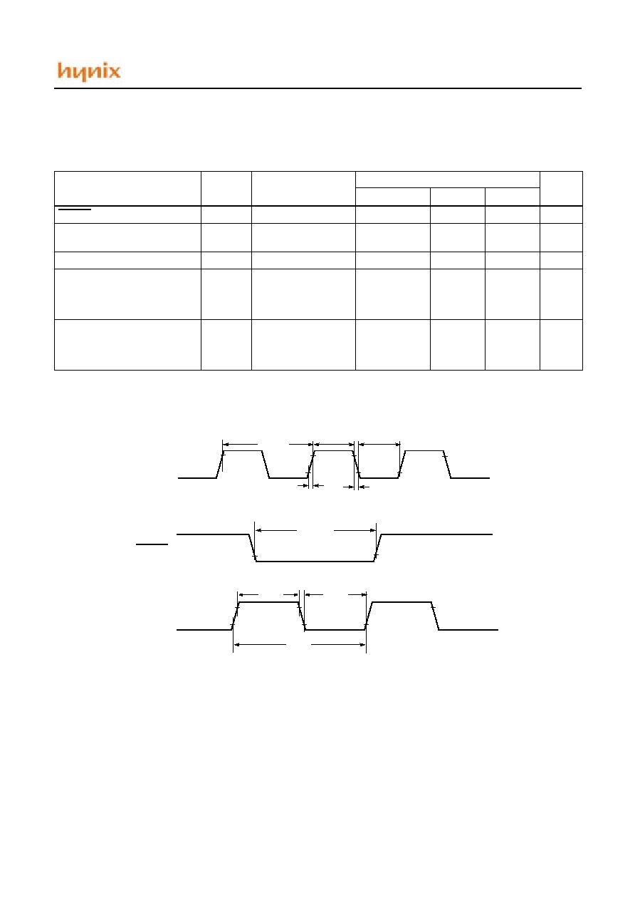
7.5 AC Electrical Characteristics (1)
· (T
A
=-40
°
°
°
°
C~+85
°
°
°
°
C)
Parameter
Symbol
Test Condition
Specification
Unit
Min
Typ
Max
External Clock Input
Frequency
F
XIN
XT osc mode
DC
-
4.0
MHz
HF osc mode
DC
-
20
MHz
LF osc mode
DC
-
200
KHz
Oscillator Frequency
1
1.
This parameter is characterized but not tested.
F
XIN
RC osc mode
DC
-
4.0
MHz
XT osc mode
0.1
-
4.0
MHz
HF osc mode
4.0
-
20
MHz
LF osc mode
5.0
-
200
KHz
External Clock Input
Period
T
XIN
XT osc mode
250
-
-
nS
HF osc mode
50
-
-
nS
LF osc mode
5
-
-
uS
Oscillator Period
1
T
XIN
RC osc mode
250
-
4.0
MHz
XT osc mode
250
-
10,000
nS
HF osc mode
50
-
250
nS
LF osc mode
5
-
200
uS
Clock in X
IN
Pin
1
Low to High Time
T
XIN
L
T
XIN
H
XT osc mode
85
-
-
nS
HF osc mode
20
-
-
nS
LF osc mode
2
-
-
uS
Clock in X
IN
Pin
1
Rise or Fall Time
T
XIN
R
T
XIN
F
XT osc mode
-
-
25
nS
HF osc mode
-
-
25
nS
LF osc mode
-
-
50
nS
GMS77C1000/GMS77C1001
July. 2001 Ver. 1.1
13
7.6 AC Electrical Characteristics (2)
·
(T
A
=-40
°
°
°
°
C~+85
°
°
°
°
C)
Parameter
1
1.
These parameters are characterized but not tested.
Symbol
Test Condition
Specification
Unit
Min
Typ
2
2.
Data in "Typ" column is at 25
°
C unless otherwise stated. These parameters are for design guidance only and are not tested.
Max
RESET Pulse Width (Low)
T
RESET
V
DD
= 5V
100
-
-
nS
Watchdog Timer Time-Out
Period ( No-prescaler )
T
WDT
V
DD
= 5V
10
14
20
mS
Internal Reset Timer Period
T
IRT
V
DD
= 5V
5
7
10
mS
EC0 High or Low Pulse Width
T
EC0
H
T
EC0
L
T
CY
= 4 X T
XIN
nS
No Prescaler
10
-
-
With Prescaler
0.5T
CY
+ 20
-
-
EC0 Period
T
EC0
P
N
= Prescaler Value
( 1,2,4,......256 )
nS
No Prescaler
20
-
-
With Prescaler
(T
CY
+40) / N
-
-
T
XIN
R
X
IN
EC0
0.15V
0.85V
DD
0.15V
DD
RESET
0.15V
DD
0.85V
DD
T
EC0
H
T
XIN
T
RESET
T
XIN
F
T
XIN
H
T
XIN
L
T
EC0
H
T
EC0
P
GMS77C1000/GMS77C1001
14
July. 2001 Ver. 1.1
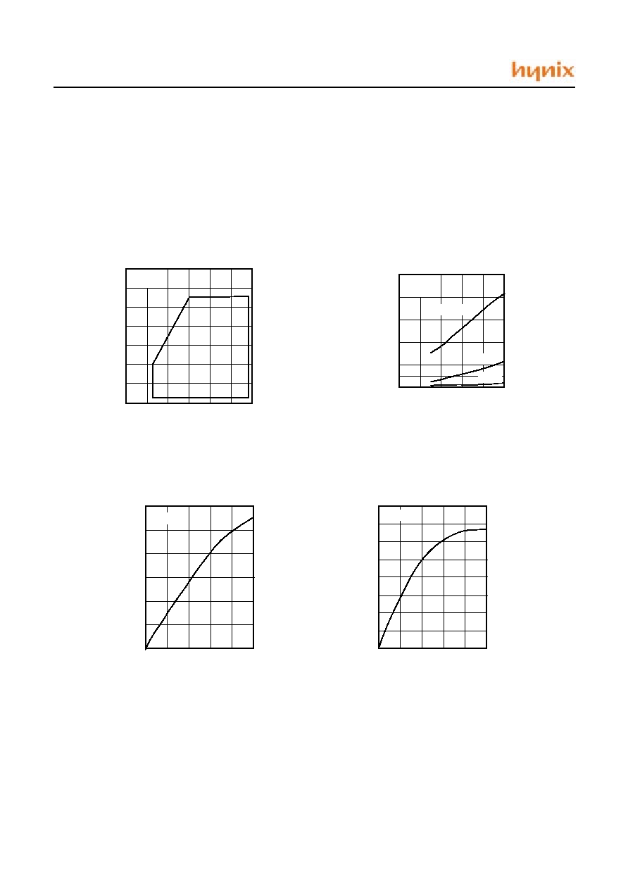
7.7 Typical Characteristics
These graphs and tables are for design guidance only and
are not tested or guaranteed.
In some graphs or tables the data presented are out-
side specified operating range (e.g. outside specified
V
DD
range). This is for information only and devices
are guaranteed to operate properly only within the
specified range.
The data is a statistical summary of data collected on units
from different lots over a period of time. "Typical" repre-
sents the mean of the distribution while "max" or "min"
represents (mean + 3
) and (mean
-
3
) respectively
where
is standard deviation
Ta= 25
°
C
Ta=25
°
C
I
DD
-
V
DD
4
3
2
1
0
(mA)
I
DD
2
3
4
5
6
V
DD
(V)
Normal Operation
16
12
8
4
0
(MHz)
f
XIN
2
3
4
5
6
V
DD
(V)
Operating Area
4MHz
24
f
XIN
= 20MHz
20
32KHz
I
OL
-
V
OL
, V
DD
=5V
32
24
16
8
0
(mA)
I
OL
V
OL
(V)
0.4
0.8
1.2
1.6
2.0
40
I
OL
-
V
OL
, V
DD
=3V
18
12
6
0
(mA)
I
OL
V
OL
(V)
0.4
0.8
1.2
1.6
2.0
Ta=25
°
C
Ta=25
°
C
GMS77C1000/GMS77C1001
July. 2001 Ver. 1.1
15
I
OH
-
V
OH
, V
DD
=5V
-16
-12
-8
-4
0
(mA)
I
OH
0.5
1.0
1.5
V
DD
-V
OH
(V)
-20
I
OH
-
V
OH
, V
DD
=3V
-6
-4
-2
0
(mA)
I
OH
0.5
1.0
1.5
-8
2.0
V
DD
-V
OH
(V)
Typical RC Oscillator
4.5
3.0
1.5
0
(MHz)
F
OSC
2.5
3
4
5
6
V
DD
(V)
Frequency
VS
. V
DD
7.5
6.0
3.5
4.5
5.5
Ta=25
°
C
R=3.3K
R=5K
R=10K
R=100K
Typical RC Oscillator
3.0
2.5
2.0
0
(MHz)
F
OSC
2.5
3
4
5
6
V
DD
(V)
Frequency
VS
. V
DD
4.5
3.5
3.5
4.5
5.5
R=3.3K
R=10K
0.5
1.0
1.5
R=5K
Typical RC Oscillator
1.50
1.25
1.00
0
(MHz)
F
OSC
2.5
3
4
5
6
V
DD
(V)
Frequency
VS
. V
DD
2.00
1.75
3.5
4.5
5.5
R=3.3K
R=10K
0.25
0.50
0.75
R=5K
Cext=0pF
Ta=25
°
C
Cext=20pF
Ta=25
°
C
Cext=100pF
4.0
R=100K
R=100K
Typical RC Oscillator
0.6
0.5
0.4
0
(MHz)
F
OSC
2.5
3
4
5
6
V
DD
(V)
Frequency
VS
. V
DD
0.8
0.7
3.5
4.5
5.5
R=3.3K
R=10K
0.1
0.2
0.3
R=5K
Ta=25
°
C
Cext=300pF
R=100K
Ta=25
°
C
Ta=25
°
C
GMS77C1000/GMS77C1001
16
July. 2001 Ver. 1.1
Cext
Rext
Average
Fosc @ 5V,25
°
C
0pF
3.3K
7.48MHz
5K
6.36MHz
10K
4.04MHz
100K
529KHz
20pF
3.3K
4.60MHz
5K
3.62MHz
10K
2.14MHz
100K
249KHz
100pF
3.3K
1.75MHz
5K
1.31MHz
10K
734KHz
100K
80KHz
300pF
3.3K
702KHz
5K
510KHz
10K
283KHz
100K
30KHz
Table 7-1 RC Oscillator Frequencies
GMS77C1000/GMS77C1001
July. 2001 Ver. 1.1
17
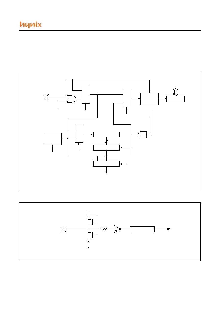
8. ARCHITECTURE
8.1 CPU Architecture
The GMS700 core is a RISC-based CPU and uses a modi-
fied Harvard architecture. This architecture uses two sepa-
rate memories with separate address buses, one for the
program memory and the other for the data memory. This
architecture adapts 33 single word instructions that are 12-
bit wide instruction and has an internal 2-stage pipeline
(fetch and execute), which results in execution of one in-
struction per single cycle(200ns @ 20MHz) except for pro-
gram branches.
The GMS77C100X can address 1K x 12 Bits program
memory and 25 Bytes data memory. And it can directly or
indirectly address data memory.
The GMS700 core has three special function registers -
PC, STATUS and FSR - in data memory map and has ATU
(Address Translation Unit) to provide address for data
memory and has an 8-bit general purpose ALU and work-
ing register(W) as an accumulator. The W register consists
of 8-bit register and it can not be an addressed register.
FIGURE 8-1 GMS700 CPU BLOCK DIAGRAM
Instruction
Decode
&
Control
Unit
STATUS
FSR
W
ALU
Instruction
Program Memory Address
Immediate Data
Data Bus
Data Memory Bus
Indirect Address
Address Translation
Unit
PC with 2-level Stack
Control
Signals
ALU
Status
GMS77C1000/GMS77C1001
18
July. 2001 Ver. 1.1
9. MEMORY
The GMS77C1000/1001 has separate memory maps for
program memory and data memory. Program memory can
only be read, not written to. It can be up to 1K words of
program memory. Data memory can be read and written to
32 bytes including special function registers.
9.1 Program Memory
The program memory is organized as 0.5K, 12-bit wide
w o r d s ( G M S 7 7 C 1 0 0 0 ) a n d 1 K , 1 2 - b i t w i d e
words(GMS77C1001). The program memory words are
addressed sequentially by a program counter. Increment-
i n g a t l o c a t i o n 1 F F
H
( G M S 7 7 C 1 0 0 0 ) o r 3 F F
H
(GMS77C1001) will cause a wrap around to 000
H
.
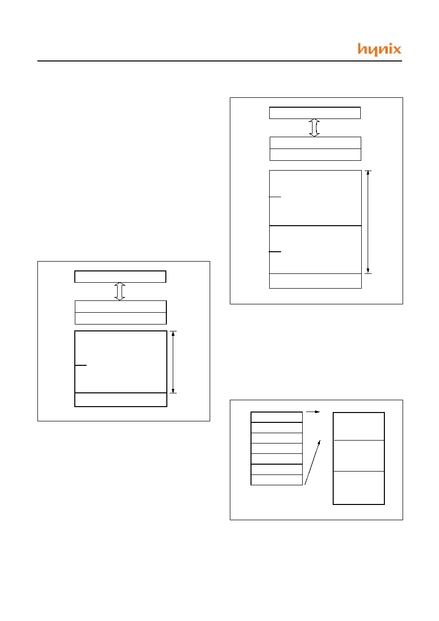
Figure 9-1 and Figure 9-2 show a map of program memo-
ry. After reset, CPU begins execution from reset vector
which is stored in address(1FF
H
: GMS77C1000, 3FF
H
:
GMS77C1001).
9.2 Data Memory
The data memory consists of 25 bytes of RAM and seven
special function registers. The data memory locations are
addressed directly or indirectly by using FSR.
Figure 9-3 shows a map of data memory. The special func-
tion registers are mapped into the data memory..
FIGURE 9-1 GMS77C1000 PROGRAM MEMORY MAP
AND STACK
PC<8:0>
Stack Level 1
Stack Level 2
Reset Vector
On-chip
Program
Memory
000
H
0FF
H
100
H
1FF
H
User Mem
o
ry
S
pace
FIGURE 9-2 GMS77C1001 PROGRAM MEMORY MAP
AND STACK
FIGURE 9-3 GMS77C1000/1 DATA MEMORY MAP
PC<9:0>
Stack Level 1
Stack Level 2
Reset Vector
On-chip
Program
Memory
000
H
0FF
H
100
H
3FF
H
User
M
e
mory
Spac
e
On-chip
Program
Memory
2FF
H
300
H
1FF
H
200
H
(Page 0)
(Page 1)
0F
H
10
H
1F
H
INDF
TMR0
PCL
STATUS
FSR
RA
RB
00
H
01
H
02
H
03
H
04
H
05
H
06
H
File Address
Special
F u n c tio n
Registers
00
H
06
H
07
H
DATA
MEMORY
(SRAM)
DATA
MEMORY
(SRAM)
GMS77C1000/GMS77C1001
July. 2001 Ver. 1.1
19
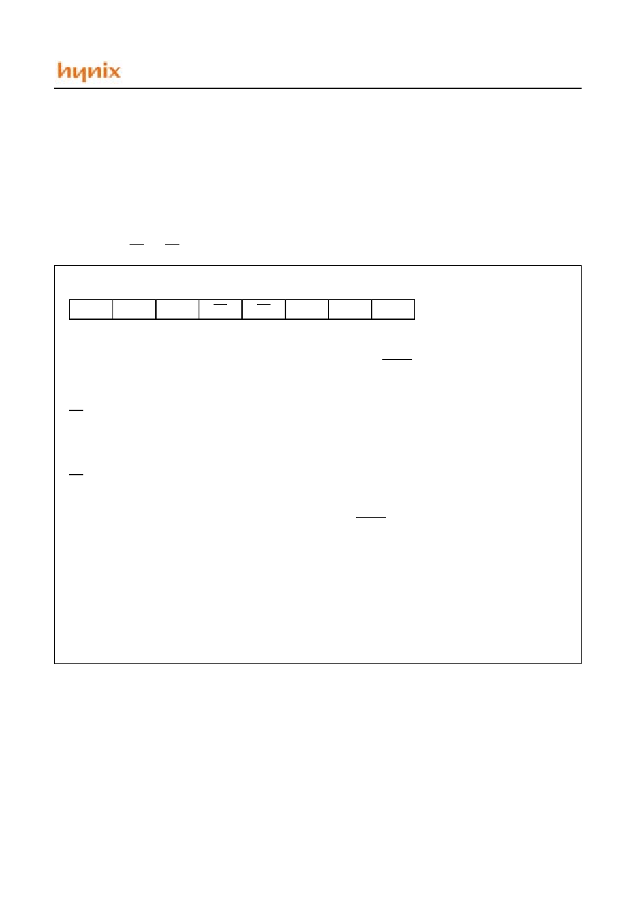
9.3 Special Function Registers
This devices has seven special function register that are the
INDF register, the Program Counter(PC), the STATUS
register, File Select Register(FSR), 8-bit Timer(TMR0),
and I/O data register(RA, RB).
The Special Function Registers are registers used by the
CPU and peripheral functions to control the operation of
the device (Table 9-1).
TMR0, RA and RB are not in the G700 CPU. They are lo-
cated in each peripheral function blocks. All special func-
tion register are placed on data memory map. The INDF
register is not a physical register and this register is used
for indirect addressing mode...
Legend : Shaded boxes = unimplemented or unused, - = unimplemented, read as `0'
x = unknown, u = unchanged, q = see the tables in Section 17 for possible values.
9.3.1 INDF Register
The INDF register is not physically implemented register,
used for indirect addressing mode. If the INDF register
are accessed, CPU goes to indirect addressing mode. Then
CPU accesses the Data memory which address is the con-
tents of FSR.
If the INDF register are accessed in indirect addressing
mode(I.e., FSR=00H), 00H will be loaded into data bus.
This time, note the arithmetic status bits of STATUS reg-
ister may be affected.
The FSR<4:0> bits are used to select data memory ad-
dresses 00
H
to 1F
H
.
GMS77C1000 and GMS77C1001 do not use banking.
FSR<7:5> are unimplemented and read as '1's.
Name
Address
Bit7
Bit6
Bit5
Bit4
Bit3
Bit2
Bit1
Bit0
Power-On
Reset
RESET and
WDT Reset
TRIS
N/A
I/O control registers (TRISA, TRISB)
1111 1111
1111 1111
OPTION
N/A
Contains control bits to configure Timer0, Timer0/WDT
prescaler and PFD
0011 1111
0011 1111
INDF
00
H
Uses contents of FSR to address data memory (not a
physical register)
xxxx xxxx
uuuu uuuu
TMR0
01
H
8-bit real-time clock/counter
xxxx xxxx
uuuu uuuu
PCL
02
H
Low order 8bits of PC
1111 1111
1111 1111
STATUS
03
H
-
-
PA0
TO
PD
Z
DC
C
0001 1xxx
000q quuu
FSR
04
H
Indirect data memory address pointer
1xxx xxxx
1uuu uuuu
RA
05
H
-
-
-
-
RA3
RA2
RA1
RA0
---- xxxx
---- uuuu
RB
06
H
RB7
RB6
RB5
RB4
RB3
RB2
RB1
RB0
xxxx xxxx
uuuu uuuu
TABLE 9-1 SPECIAL FUNCTION REGISTER SUMMARY
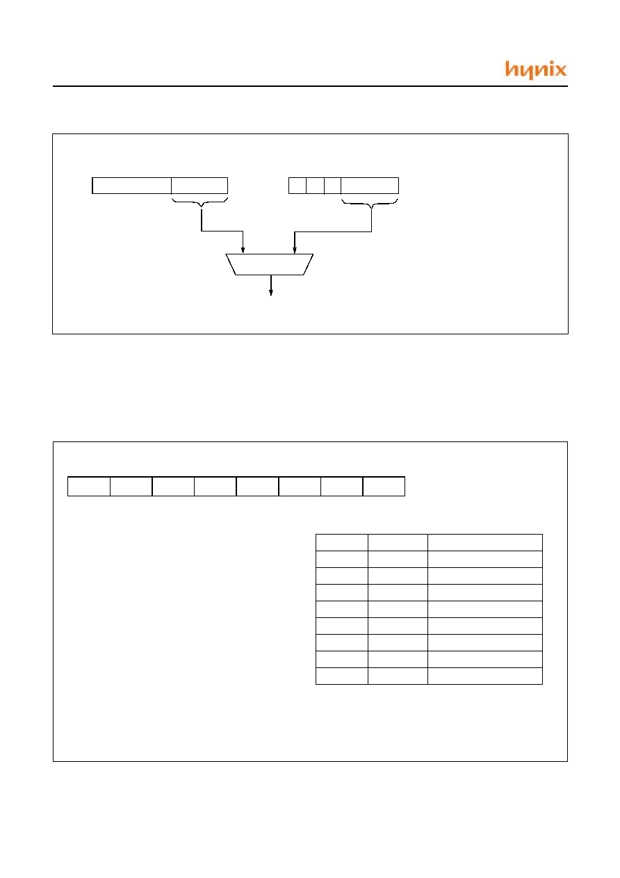
FIGURE 9-4 DIRECT/INDIRECT ADDRESSING
4
0
4
0
(opcode)
(FSR)
location
select
location
select
Data
Memory
00
H
0F
H
10
H
1F
H
Direct Addressing
Indirect Addressing
GMS77C1000/GMS77C1001
20
July. 2001 Ver. 1.1
9.3.2 TMR0 Register
The TMR0 register is a data register for 8-bit timer/
counter. In reset state, the TMR0 register is initialized with
"00
H
".
9.3.3 Program Counter (PC)
The program counter contains the 10-bit address of the in-
struction to be executed(9-bit address for GMS77C1000).
The lower 8 bits of the program counter are contained in
the PCL register which can be provided by the instruction
word for a call instruction, or any instruction where the
PCL is the destination while the ninth bit of the program
counter comes from the page address bit - PA0 of the STA-
TUS register(GMS77C1001 only).
This is necessary to cause program branches across pro-
gram memory page boundaries.
Prior to the execution of a branch operation, the user must
initialize the PA0 bit of STATUS register.
The eighth bit of the program counter can come from the
instruction word by execution of goto instruction, or can be
cleared by execution of call or any instruction where the
PCL is the destination.
In reset state, the program counter is initialized with
"1FF
H
"(GMS77C1000) or "3FF
H
"(GMS77C1001).
Note: Because PC<8> is cleared in the subroutine call
in-
struction, or any Modify PCL instruction, all subrou-
tine calls or computed jumps are limited to the first
256 locations of any program memory page (512
words long).
9.3.4 Stack Operation
The GMS77C1000/1001 have a 2-level hardware stack.
The stack register consists of two 9-bit save regis-
ters(GMS77C1000), 10-bit save registers(GMS77C1001).
A physical transfer of register contents from the program
counter to the stack or vice versa, and within the stack, oc-
curs on call and return instructions. If more than two se-
quential call instructions are executed, only the most recent
two return address are stored. If more than two sequential
return instructions are executed, the stack will be filled
with the address previously stored in level 2. The stack
cannot be read or written by program.
jump instrunciton
subroutine call instruction
FIGURE 9-5 LOADING OF BRANCH INSTRUCTION -
GMS77C1000
PCL
PC
8
0
Instruction Word
PCL
PC
8
7
0
Instruction Word
Reset to `0'
jump instruction
subroutine call Instruction
FIGURE 9-6 LOADING OF BRANCH INSTRUCTION -
GMS77C1001
FIGURE 9-7 OPERATION OF 2-LEVEL STACK
PCL
PC
8
0
Instruction Word
9
PA0
PCL
PC
8
7
0
Instruction Word
9
PA0
Reset to `0'
PC
STACK LEVEL1
STACK LEVEL2
0
9(8)
return
return
subroutine call
GMS77C1001(GMS77C1000)
subroutine call
GMS77C1000/GMS77C1001
July. 2001 Ver. 1.1
21
9.3.5 STATUS Register
This register contains the arithmetic status of the ALU, the
RESET status, and the page select bit for program memo-
ries larger than 512 words.
The STATUS register can be the destination for any in-
struction, as with any other register. If the STATUS regis-
ter is the destination for an instruction that affects the Z,
DC or C bits, then the write to these three bits is disabled.
These bits are set or cleared according to the device logic.
Furthermore, the TO and PD bits are not writable. There-
fore, the result of an instruction with the STATUS register
as destination may be different than intended.
It is recommended that only instructions that do not affect
status of CPU be used on STATUS register. Care should be
exercised when writing to the STATUS register as the
ALU status bits are updated upon completion of the write
operation, possibly leaving the STATUS register with a re-
sult that is different than intended. In reset state, the STA-
TUS register is initialized with "00011XXX
B
".
9.3.6 FSR Register
The FSR register is an 8-bit register. The lower 5 bits are
used to store indirect address for data memory. The upper
3 bits are unimplemented and read as "0". Figure 9-9
shows how the FSR register can be used in indirect ad-
dressing mode.
In reset state, the FSR register is initialized with
"1XXX_XXXX
B
".
FIGURE 9-8 STATUS REGISTER
-
PA0
R/W
TO
R
PD
R
Z
R/W
DC
R/W
C
R/W
bit7
bit0
PA0: Program memory page select bits
0 = page 0 (000h - 1FFh) - GMS77C1000/1001
1 = page 1 (200h - 3FFh) - GMS77C1001
TO: Time-overflow bit
1 = After power-up, watchdog clear instruction, or
entering power-down mode
0 = A watchdog timer time-overflow occurred
PD: Power-down bit
1 = After power-up or by the watchdog clear
instruction
0 = By execution of power-down mode
Z: Zero bit
1 = The result of an arithmetic or logic operation
is zero
0 = The result of an arithmetic or logic operation
is not zero
DC: Digit carry/borrow bit
(for addition and subtraction)
addition
1 = A carry from the 4th low order bit of the result
occurred
0 = A carry from the 4th low order bit of the result
did not occur
subtraction
1 = A borrow from the 4th low order bit of the
result did not occur
0 = A borrow from the 4th low order bit of the
result occurred
C: Carry/borrow bit
(for additon,subtraction and rotation)
addition
1 = A carry occurred
0 = A carry did not occur
subtraction
1 = A borrow did not occur
0 = A borrow occurred
rotation
Load bit with LSB or MSB, respectively
R = Readable bit
W = Writable bit
ADDRESS ; 03
H
RESET VALUE : 0001_1XXX
-
GMS77C1000/GMS77C1001
22
July. 2001 Ver. 1.1
9.3.7 OPTION Register
The OPTION register consists of 8-bit write-only register
and can not addressed. This register is able to control the
status of PFD, TMR0/WDT prescaler and TMR0.
To modify the OPTION register, the content of W register
are transferred to the OPTION register by executing the
OPTION instruction.
In reset state, the OPTION register is initialized with
"00111111
B
" .
FIGURE 9-9 FSR REGISTER AND DIRECT/INDIRECT ADDRESSING MODE
FSR
Address : 04H
8
0
11
5
0
4
4
-
-
-
1
0
Indirect Addressing mode
Direct Addressing mode
Data Memory Address
Instruction Word
OPCODE
RESET Value: 1XXX_XXXX
B
FIGURE 9-10 OPTION REGISTER
LOWOPT
W
PFDEN
W
T0CS
W
T0SE
W
PSA
W
PS2
W
PS1
W
PS0
W
bit7
6
bit0
5
4
3
2
1
LOWOPT: Power-fail detection level select bit.
1 = Lowered detection level (2.5V @ 5V)
0 = Normal detection level (3V @ 5V)
PFDEN: Power-fail detection enable bit
1 = Enable power-fail detection
0 = Disable power-fail detection
T0CS: Timer 0 clock source select bit
1 = Transition on EC0 pin
0 = Internal instruction cycle clock
T0SE: Timer 0 source edge select bit
1 = Increment on high-to-low transition on
EC0
0 = Increment on low-to-high transition on
EC0
PSA: Prescaler assignment bit
1 = Prescaler assigned to the WDT
0 = Prescaler assigned to the Timer 0
PS2-PS0: Prescaler rate select bits)
Bit Value
Timer 0 rate
WDT rate
000
1:2
1:2 (Typ. 28mS)
001
1:4
1:4 (Typ. 56mS)
010
1:8
1:8 (Typ. 112mS)
011
1:16
1:16 (Typ. 224mS)
100
1:32
1:32 (Typ. 448mS)
101
1:64
1:64 (Typ. 896mS)
110
1:128
1:128 (Typ. 1792mS)
111
1:256
1:256 (Typ. 3584mS)
W = Writable bit
-n = Value at POR reset
ADDRESS ; 03
H
RESET VALUE : 0011_1111
GMS77C1000/GMS77C1001
July. 2001 Ver. 1.1
23
10. I/O PORTS
The GMS77C1000/1001 has a 4-bit I/O port(RA) and a 8-
bit I/O port(RB).
All pin have data(RA,RB) and direction(TRISA,TRISB)
registers which can assign these ports as output or input.
A "0" in the port direction registers configure the corre-
sponding port pin as output. Conversely, write "1" to the
corresponding bit to specify it as input pin (Hi-Z state).
For example, to use the even numbered bit of RB as output
ports and the odd numbered bits as input ports, write "55
H
"
to TRISB register during initial setting as shown in Figure
10-1.
All the port direction registers in the GMS77C1000/1001
have "1" written to them by reset function. This causes all
port as input.
10.1 Port RA
RA is a 4-bit I/O register. Each I/O pin can independently
used as an input or an output through the port direction reg-
ister, TRISA. A "0" in the TRISA register configure the
corresponding port pin as output. Conversely, write "1"to
the corresponding bit to specify it as input pin.
Bits 7-4 are unimplemented and read as '0's.
10.2 Port RB
RB is an 8-bit I/O register. Each I/O pin can independently
used as an input or an output through the port direction reg-
ister, TRISB. A "0" in the TRISB register configure the
corresponding port pin as output. Conversely, write "1"to
the corresponding bit to specify it as input pin.
Note: A read of the ports reads the pins, not the output
data latches. That is, if an output driver on a pin is
enabled and driven high, but the external system is
holding it low, a read of the port will indicate that the
pin is low.
10.3 I/O Interfacing
The equivalent circuit for an I/O port pin is shown in Fig-
ure 10-4. All ports may be used for both input and output
operation.
For input operations these ports are non-latching. Any in-
put must be present until read by an input instruction. The
outputs are latched and remain unchanged until the output
latch is rewritten. To use a port pin as output, the corre-
sponding direction control bit (in TRISA, TRISB) must be
cleared (= 0). For use as an input, the corresponding TRIS
bit must be set. Any I/O pin can be programmed individu-
ally as input or output..
10.4 I/O Successive Operations
The actual write to an I/O port happens at the end of an in-
struction cycle, whereas for reading, the data must be valid
at the beginning of the instruction cycle (Figure 10-5).
Therefore, care must be exercised if a write followed by a
read operation is carried out on the same I/O port.
The sequence of instructions should allow the pin voltage
to stabilize (load dependent) before the next instruction,
which causes that file to be read into the CPU, is executed.
FIGURE 10-1 EXAMPLE OF PORT I/O ASSIGNMENT
FIGURE 10-2 RA PORT REGISTERS
0
PORT RB
7
1
6
0
5
1
4
0
3
1
2
0
1
1
0
O U T IN O U T IN O U T IN O U T IN
Write "55
H
" to port RB direction register
TRISB
RA
R A 3
3
R A 2
2
R A 1
1
R A 0
0
RA Data Register
RA Direction Register
TRISA
ADDRESS : 05
H
RESET VALUE : Undefined
ADDRESS : N/A
RESET VALUE : 0F
H
FIGURE 10-3 RB PORT REGISTERS
RB
R B 7
7
R B 6
6
R B 5
5
R B 4
4
RB Data Register
RB Direction Register
TRISB
ADDRESS : 06
H
RESET VALUE : Undefined
ADDRESS : N/A
RESET VALUE : FF
H
R B 3
3
R B 2
2
R B 1
1
R B 0
0
GMS77C1000/GMS77C1001
24
July. 2001 Ver. 1.1
Otherwise, the previous state of that pin may be read into
the CPU rather than the new state.
When in doubt, it is better to separate these instructions
with a NOP or another instruction not accessing this I/O
port.
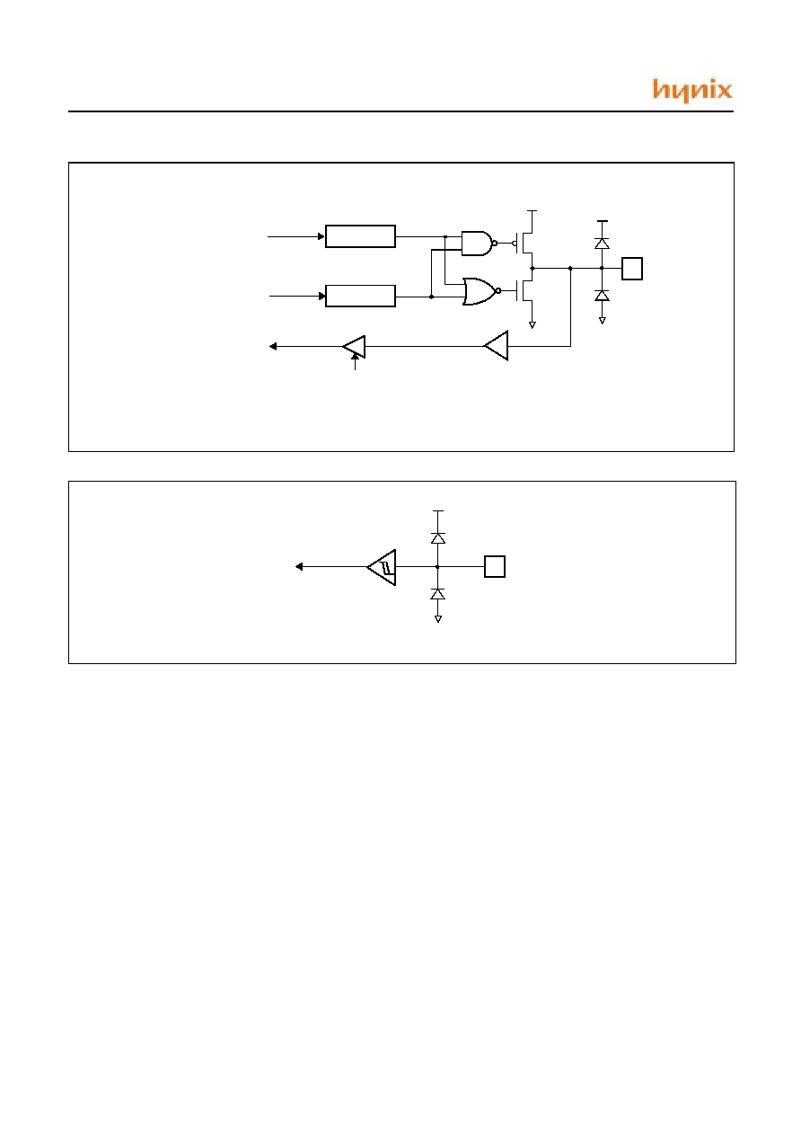
FIGURE 10-4 EQUIVALENT CIRCUIT FOR A SINGLE I/O PIN
Name
Address
Bit7
Bit6
Bit5
Bit4
Bit3
Bit2
Bit1
Bit0
Power-On
Reset
RESET and
WDT Reset
TRIS
N/A
I/O control registers (TRISA, TRISB)
1111 1111
1111 1111
RA
05
H
-
-
-
-
RA3
RA2
RA1
RA0
---- xxxx
---- uuuu
RB
06
H
RB7
RB6
RB5
RB4
RB3
RB2
RB1
RB0
xxxx xxxx
uuuu uuuu
TABLE 10-1 SUMMARY OF PORT REGISTERS
Legend: Shaded boxes = unimplemented or unused, - = unimplemented, read as `0', x = unknown, u = unchanged.
Data Bus
Data Bus
Data Bus
Data Reg.
Direction Reg.
Read
V
DD
V
SS
FIGURE 10-5 SUCCESSIVE I/O OPERATION
output RB
PC
RB7:RB0
Instruction
This example shows a write
fetched
Q1 Q2 Q3 Q4 Q1 Q2 Q3 Q4 Q1 Q2 Q3 Q4 Q1 Q2 Q3 Q4
PC+1
PC+2
PC+3
read RB port
no operation
no operation
Port pin
written here
Port pin
read here
to RB followed by a read
from RB.
GMS77C1000/GMS77C1001
July. 2001 Ver. 1.1
25
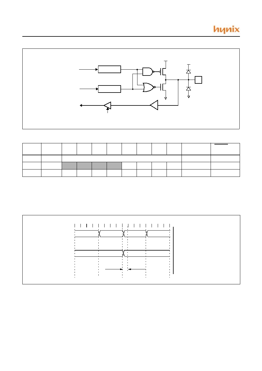
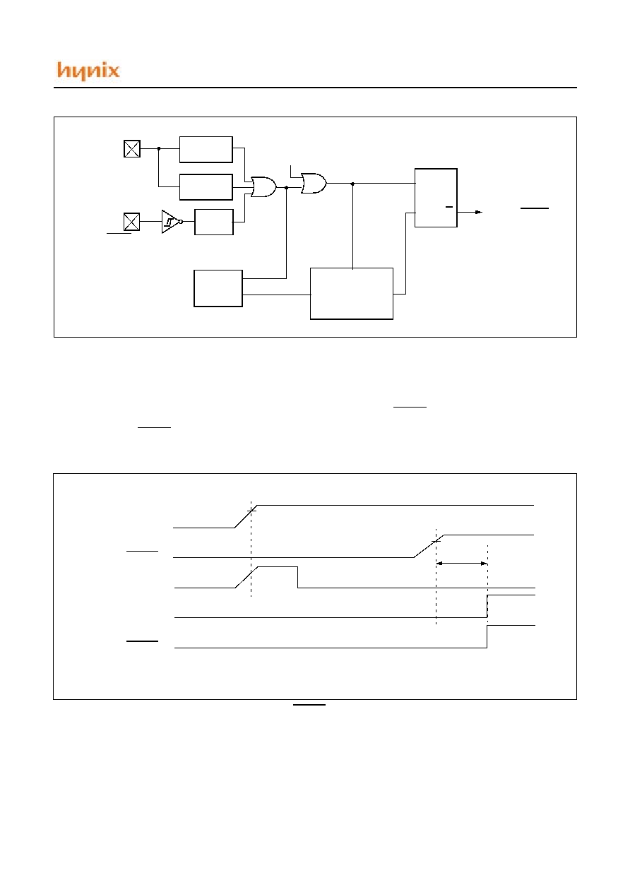
11. TIMER0 MODULE AND TMR0 REGISTER
The Timer0 module has the following features:
·
8-bit timer/counter register, TMR0
· 8-bit software programmable prescaler
· Internal or external clock select
· Edge select for external clock
Figure 11-1 is a simplified block diagram of the Timer0
module, while Figure 11-2 shows the electrical structure of
the Timer0 input
.
FIGURE 11-1 BLOCK DIAGRAM OF THE TIMER0/WDT PRESCALER
FIGURE 11-2 ELECTRICAL STRUCTURE OF EC0 PIN
T
CY
( = F
OSC
/4)
1
8-bit Prescaler
EC0
pin
0
Sync with
Internal
Clocks
TMR0 reg
8
Data bus
(2cycle delay)
T0SE
8
T0CS
MUX
0
1
MUX
1
0
PSA
MUX
8 - to - 1 MUX
Watchdog
Timer
MUX
PS2:PS0
PSA
PSA
1
0
WDT Time-Out
WDT Enable bit
clear
ECO
P
N
pin
R
IN
Schmitt Trigger
Input Buffer
(1)
Note 1: ESD protection circuits
Noise Filter
GMS77C1000/GMS77C1001
26
July. 2001 Ver. 1.1
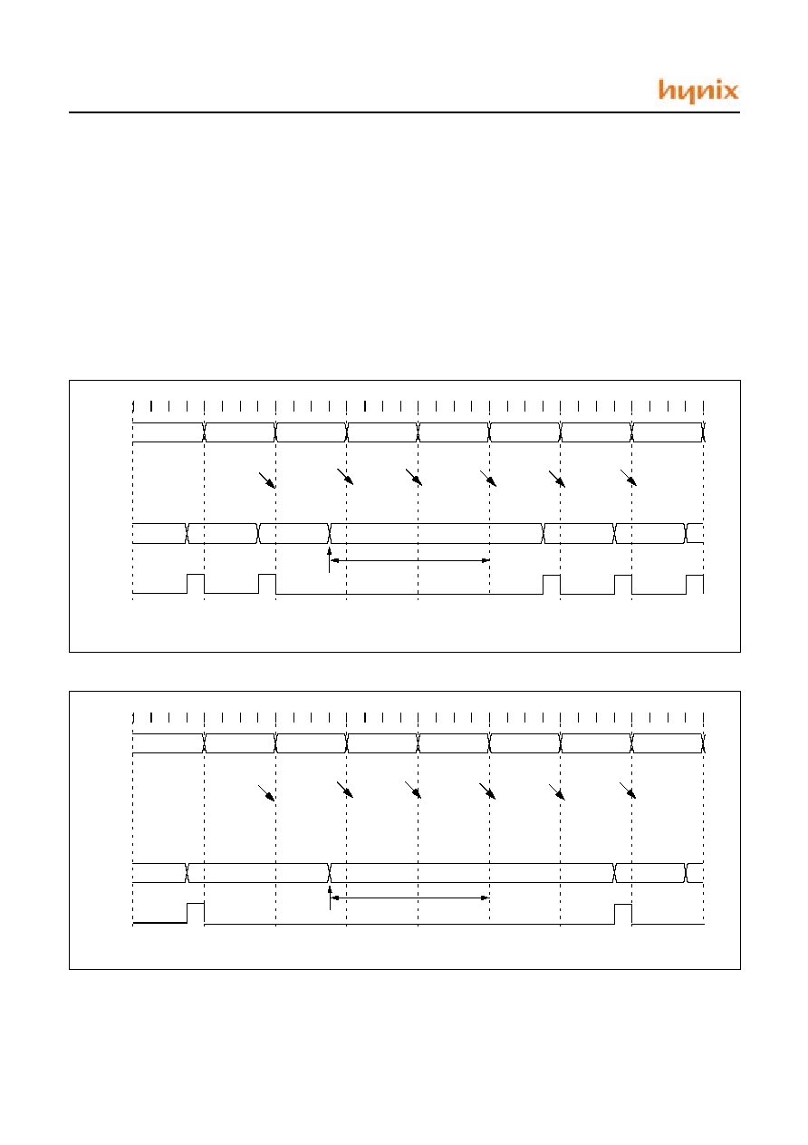
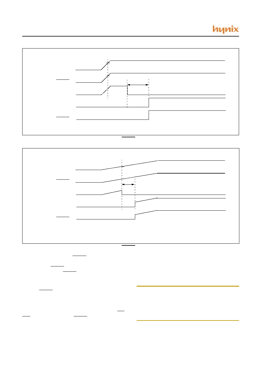
11.1 Timer Mode
If the OPTION register bit5(T0CS) is cleared, the timer
mode is selected and is operated with internal system clock
(T
CY
). The Timer0 module will increment every instruc-
tion cycle (without prescaler). If TMR0 register is written,
the increment is inhibited for the following two cycles. The
user can work around this by writing an adjusted value to
the TMR0 register.
Figure 11-3 and Figure 11-4 show the timing diagram of
Timer.
- No Prescaler (PSA=0)
Timer will increment every instruction cycle(Q4).
- With Prescaler (PSA=1)
Timer will increment with prescaler division ratio.
@ PS2~PS0 = (1:2) ~ (1:256)Counter Mode
11.2 Counter Mode
If the OPTION register bit5(T0CS) is set, the counter
mode is selected and operates with event clock input.
In this mode, Timer0 will increment either on every rising
or falling edge of pin EC0. The incrementing edge is deter-
mined by the source edge select bit T0SE (OPTION<4>).
Clearing the T0SE bit selects the rising edge.
FIGURE 11-3 TIMER0 TIMING: INTERNAL CLOCK/NO PRESCALE
FIGURE 11-4 TIMER0 TIMING: INTERNAL CLOCK/PRESCALER 1:2
[ W
'
TMR0 ]
PC-1
TMR0
Instruction
Fetch
Q1 Q2 Q3 Q4
PC
Q1 Q2 Q3 Q4
PC+1
Q1 Q2 Q3 Q4
PC+2
Q1 Q2 Q3 Q4
PC+3
Q1 Q2 Q3 Q4
PC+4
Q1 Q2 Q3 Q4
PC+5
Q1 Q2 Q3 Q4
PC+6
Q1 Q2 Q3 Q4
[ TMR0
'
W ]
[ TMR0
'
W ]
[ TMR0
'
W ]
[ TMR0
'
W ]
[ TMR0
'
W ]
T0
T0+1
T0+2
NT0
NT0+1
NT0+2
Write TMR0
executed
Read TMR0
reads NT0
Read TMR0
reads NT0
Read TMR0
reads NT0
Read TMR0
reads NT0+1
Read TMR0
reads NT0+2
PC
(Program
Counter)
Instruction
Executed
increment inhibited
Timer0
Clock
[ W
'
TMR0 ]
PC-1
TMR0
Instruction
Fetch
Q1 Q2 Q3 Q4
PC
Q1 Q2 Q3 Q4
PC+1
Q1 Q2 Q3 Q4
PC+2
Q1 Q2 Q3 Q4
PC+3
Q1 Q2 Q3 Q4
PC+4
Q1 Q2 Q3 Q4
PC+5
Q1 Q2 Q3 Q4
PC+6
Q1 Q2 Q3 Q4
[ TMR0
'
W ]
[ TMR0
'
W ]
[ TMR0
'
W ]
[ TMR0
'
W ]
[ TMR0
'
W ]
T0
T0+1
NT0
NT0+1
PC
(Program
Counter)
increment inhabited
Timer0
Clock
Write TMR0
executed
Read TMR0
reads NT0
Read TMR0
reads NT0
Read TMR0
reads NT0
Read TMR0
reads NT0+1
Read TMR0
reads NT0+2
Instruction
Executed
GMS77C1000/GMS77C1001
July. 2001 Ver. 1.1
27
Legend: x = unknown, u = unchanged.
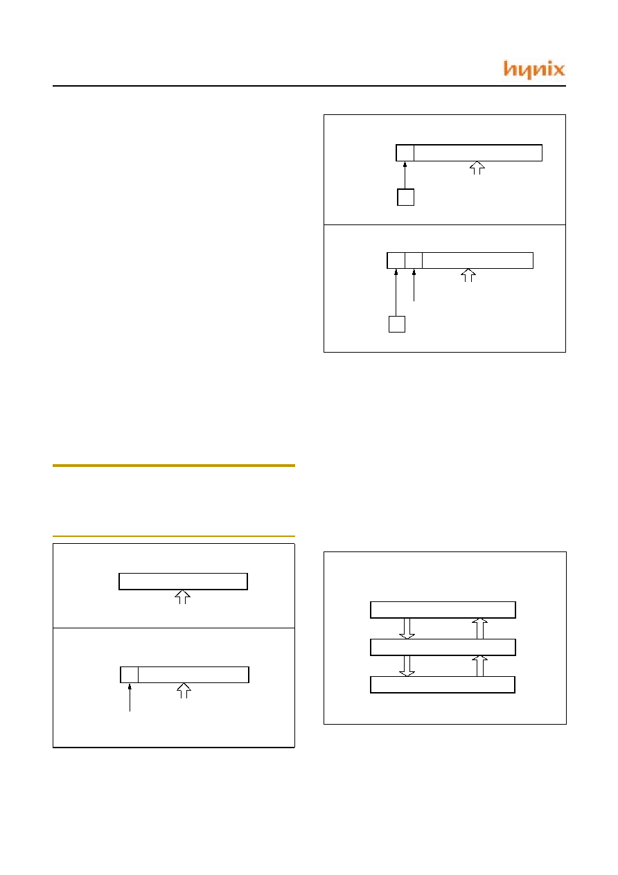
11.3 Using Timer0 with an External Clock
When an external clock input is used for Timer0, it must
meet certain requirements. The external clock requirement
is due to internal phase clock (T
OSC
) synchronization. Al-
so, there is a delay in the actual incrementing of Timer0 af-
ter synchronization.
11.3.1 External Clock Synchronization
The synchronization of EC0 input with the internal phase
clocks is accomplished by sampling EC0 clock or the pres-
caler output on the Q2 and Q4 falling of the internal phase
clocks.
After the synchronization, counter increments on the next
instruction cycle (Q4). There is a small delay from the time
the external clock edge occurs to the time the Timer0 mod-
ule is actually incrementing. Figure 11-5 shows the syn-
chronization and the increment of the counter mode.
· EC0 clock specification
- No Prescaler (PSA = 0)
High or low time(min)
2T
XIN
+ 20ns
- With Prescaler (PSA = 1)
High or low time(min)
4T
XIN
+ 40ns
But, there is a noise filter on the EC0 pin, the minimum low
or high time(10ns) should be required.
11.3.2 Timer0 Increment Delay
Since the prescaler output is synchronized with the internal
clocks, there is a small delay from the time the external
clock edge occurs to the time the Timer0 module is actual-
ly incrementing. Figure 11-5 shows the delay from the ex-
ternal clock edge to the timer incrementing.
11.4 Prescaler
The prescaler may be used by either the Timer0 module or
the Watchdog Timer, but not both. Thus, a prescaler as-
signment for the Timer0 module means that there is no
prescaler for the WDT, and vice-versa.
The prescaler assignment is controlled in software by the
control bit PSA (OPTION<3>). Clearing the PSA bit will
assign the prescaler to Timer0. The prescaler is neither
readable nor writable.
The PSA and PS2:PS0 bits (OPTION<3:0>) determine
prescaler assignment and prescale ratio. When the prescal-
er is assigned to the Timer0 module, prescale values of 1:2,
Name
Address
Bit7
Bit6
Bit5
Bit4
Bit3
Bit2
Bit1
Bit0
Power-On
Reset
RESET and
WDT Reset
TMR0
01
H
8-bit real-time clock/counter
xxxx xxxx
uuuu uuuu
OPTION N/A
LOWOPT
PFDEN
T0CS
T0SE
PSA
PS2
PS1
PS0
0011 1111
0011 1111
TABLE 11-1 REGISTERS ASSOCIATED WITH TIMER0
FIGURE 11-5 TIMER0 TIMING WITH EXTERNAL CLOCK
Q1 Q2 Q3 Q4 Q1 Q2 Q3 Q4 Q1 Q2 Q3 Q4
T0
T0+1
Note 1: Delay from clock input change to TMR0 increment is 3T
XIN
to 7T
XIN
. (Duration of Q = T
XIN
).
Q1 Q2 Q3 Q4
T0+2
External Clock Input or
Prescaler Output
(2)
External Clock/Prescaler
Output After Sampling
Increment TMR0 (Q4)
TMR0
Small Pulse
misses sampling
(1)
(3)
Therefore, the error in measuring the interval between two edges on TMR0 input =
±
4T
XIN
max.
2: External clock if no prescaler selected, prescaler output otherwise.
3: The arrows indicate the points in time where sampling occurs.

GMS77C1000/GMS77C1001
28
July. 2001 Ver. 1.1
1:4,..., 1:256 are selectable.
When assigned to the Timer0 module, all instructions writ-
ing to the TMR0 register will clear the prescaler. When as-
signed to WDT, a CLRWDT instruction will clear the
prescaler along with the WDT.
On a RESET, the prescaler contains all '0's.
GMS77C1000/GMS77C1001
July. 2001 Ver. 1.1
29
12. CONFIGURATION AREA
The device configuration area can be programmed or left
unprogrammed to select device configurations such as os-
cillator type, security bit or watchdog timer enable bit.
Four memory locations [AAAH ~ (AAA+3)
H
] are desig-
nated as customer ID recording locations where the user
can store check-sum or other customer identification num-
bers. These area are not accessible during normal execu-
tion but are readable and writable during program/verify
mode. It is recommended that only the 4 least significant
bits of ID recording locations are used.
FIGURE 12-1 DEVICE CONFIGURATION AREA
bit0
3
-
ID0
bit11
4
-
ID1
-
ID2
-
ID3
AAA
H
AAA
H
+1
AAA
H
+2
AAA
H
+3
Configuration Word
FFF
H
FIGURE 12-2 CONFIGURATION WORD FOR GMS77C1000/1001
bit11
bit0
4
3
2
1
bit 3
CP : Code protection bit.
1 = Code protection disabled
0 = Code protection enabled
bit 2
WDTE: Watchdog timer enable bit
1 = WDT enabled
0 = WDT disabled
bit 1-0
FOSC1:FOSC0: Oscillator selection bits
11 = RC oscillator
10 = HF oscillator
01 = XT oscillator
00 = LF oscillator
Address
: FFF
H
CP
WDTE FOSC1 FOSC0
-
Unimplemented, read as `0'
Configuration Word
GMS77C1000/GMS77C1001
30
July. 2001 Ver. 1.1
13. OSCILLATOR CIRCUITS
GMS77C100X supports four user-selectable oscillator
modes. The oscillator modes are selected by programming
the appropriate values into the configuration word.
- XT : Crystal/Resonator
- HF : High Speed Crystal/Resonator
- LF : Low Speed and Low Power Crystal
- RC : External Resistor/Capacitor
13.1 XT, HF or LF Mode
In XT, LF or HF modes, a crystal or ceramic resonator is
connected to the X
IN
and X
OUT
pins to establish oscillation
(Figure 13-1). The GMS77C100X oscillator design re-
quires the use of a parallel cut crystal. Use of a series cut
crystal may give a frequency out of the crystal manufactur-
ers specifications. Bits 0 and 1 of the configuration register
(FOSC1:FOSC2) are used to configure the different exter-
nal resonator/crystal oscillator modes. These bits allow the
selection of the appropriate gain setting for the internal
driver to match the desired operating frequency. When in
XT, LF or HF modes, the device can have an external clock
source drive the X
IN
pin (Figure 13-2). In this case, the
X
OUT
pin should be left open.
Note: These values are for design guidance only. Since
each resonator has its own characteristics, the user
should consult the resonator manufacturer for ap-
propriate values of external components.
Note: These values are for design guidance only. Since
each crystal has its own characteristics, the user
should consult the crystal manufacturer for appropri-
ate values of external components.
If you change from this device to another device,
please verify oscillator characteristics in your
application.
13.2 RC Oscillation Mode
The external RC oscillator mode provides a cost-effective
approach for applications that do not require a precise op-
erating frequency. In this mode, the RC oscillator frequen-
FIGURE 13-1 CRYSTAL OR CERAMIC RESONATOR
(HF, XT OR LF OSC CONFIGURATION)
FIGURE 13-2 EXTERNAL CLOCK INPUT OPERATION
(HF, XT OR LF OSC CONFIGURATION)
X
OUT
X
IN
To internal
RF
(2)
SLEEP
logic
XTAL
C2
(1)
C1
(1)
Note 1: See Capacitor Selection tables for recommended
values of C1 and C2.
2: RF varies with the crystal chosen
(approx. value = 9 M
).
X
OUT
X
IN
OPEN
GMS77C100X
Clock from
ext. system
Osc
Type
Resonator
Freq
Cap.Range
C1
Cap. Range
C2
XT
455 kHz
2.0 MHz
4.0 MHz
22-100 pF
15-68 pF
15-68 pF
22-100 pF
15-68 pF
15-68 pF
HF
4.0 MHz
8.0 MHz
16.0 MHz
15-68 pF
10-68 pF
10-22 pF
15-68 pF
10-68 pF
10-22 pF
TABLE 13-1 CAPACITOR SELECTION FOR CERAMIC
RESONATORS
Osc
Type
Crystal
Freq
Cap.Range
C1
Cap. Range
C2
LF
32 kHz
1
100 kHz
200 kHZ
1.
For V
DD
> 4.5V, C1 = C2
30 pF is recommended.
15 pF
15-30 pF
15-30 pF
15 pF
30-47 pF
15-82 pF
XT
100 kHz
200 kHz
455 kHz
1 MHz
2 MHz
4 MHz
15-30 pF
15-30 pF
15-30 pF
15-30 pF
15-30 pF
15-47 pF
200-300 pF
100-200 pF
15-100 pF
15-30 pF
15-30 pF
15-47 pF
HF
4 MHz
8 MHz
20 MHz
15-30 pF
15-30 pF
15-30 pF
15-30 pF
15-30 pF
15-30 pF
TABLE 13-2 CAPACITOR SELECTION FOR CRYSTAL
GMS77C1000/GMS77C1001
July. 2001 Ver. 1.1
31
cy is a function of the supply voltage, the resistor(R) and
capacitor(C) values, and the operating temperature.
In addition, the oscillator frequency will vary from unit to
unit due to normal manufacturing process variations. Fur-
thermore, the difference in lead frame capacitance between
package types also affects the oscillation frequency, espe-
cially for low C values. The external R and C component
tolerances contribute to oscillator frequency variation as
well.
The user also needs to take into account variation due to
tolerance of external R and C components used.
Figure 13-3 shows how the R is connected to the
GMS77C100X. For Rext values below 2.2 k
, the oscilla-
tor operation may become unstable, or stop completely.
For very high Rext values (e.g., 1 M
) the oscillator be-
comes sensitive to noise, humidity and leakage. Thus, we
recommend keeping Rext between 3 k
and 100 k
. Ta-
ble 13-3 shows recommended value of Rext and Cext.
Although the oscillator will operate with no external ca-
pacitor (Cext = 0 pF), it is recommend using values above
20 pF for noise and stability reasons. With no or small ex-
ternal capacitance, the oscillation frequency can vary dra-
matically due to changes in external capacitances, such as
PCB trace capacitance or package lead frame capacitance.
The Electrical Specifications sections show R frequency
variation from part to part due to normal process variation.
Also, see the Electrical Specifications sections for variation of os-
cillator frequency due to V
DD
for given Rext/Cext values as well
as frequency variation due to operating temperature for given R,
C, and V
DD
values.
The oscillator frequency, divided by 4, is available on the
X
OUT
pin, and can be used for test purposes or to synchro-
nize other logic.
Cext
Rext
Average F
XIN
@ 5V, 25°C
0pF
3.3K
5K
10K
100K
7.48MHz
6.36MHz
4.04MHz
529KHz
20pF
3.3K
5K
10K
100K
4.60MHz
3.62MHz
2.14MHz
249KHz
100pF
3.3K
5K
10K
100K
1.75MHz
1.31MHz
734KHz
80KHz
300pF
3.3K
5K
10K
100K
702KHz
510KHz
283KHz
30KHz
TABLE 13-3 RC OSCILLATION FREQUENCIES
FIGURE 13-3 RC OSCILLATION MODE
N
R
ext
Internal
V
DD
X
IN
X
OUT
Clock
F
XIN
/4
C
ext
GMS77C1000/GMS77C1001
32
July. 2001 Ver. 1.1
14. RESET
GMS77C100X devices may be reset in one of the follow-
ing ways:
- Power-On Reset (POR)
- Power-Fail detect reset (PFDR)
- RESET (normal operation)
- RESET wake-up reset (from SLEEP)
- WDT reset (normal operation)
- WDT wake-up reset (from SLEEP)
Each one of these reset conditions causes the program
counter to branch to reset vector address. (GMS77C1000
is 1FF
H
and GMS77C1001 is 3FF
H
).
Table 14-1 shows these reset conditions for the PCL and
STATUS registers.
Some registers are not affected in any reset condition.
Their status is unknown on POR and unchanged in any
other reset. Most other registers are reset to a "reset state"
on Power-On Reset (POR), PFDR, RESET or WDT reset.
A RESET or WDT wake-up from SLEEP also results in a
device reset, and not a continuation of operation before
SLEEP.
The TO and PD bits (STATUS <4:3>) are set or cleared
depending on the different reset conditions. These bits may
be used to determine the nature of the reset.
Table 14-2 lists a full description of reset states of all reg-
isters. Figure 14-1 shows a simplified block diagram of the
on-chip reset circuit.
Condition
PCL
Addr: 02
H
STATUS
Addr: 03
H
Power-On Reset
1111 1111
0001 1xxx
RESET reset or PFD
reset (normal operation)
1111 1111
000u uuuu
1
1. TO and PD bits retain their last value until one of the other
reset conditions occur.
RESET wake-up or PFD
reset (from SLEEP)
1111 1111
0001 0uuu
WDT reset (normal
operation)
1111 1111
0000 uuuu
2
2. The CLRWDT instruction will set the TO and PD bits.
Legend : x = unknown, u = unchanged.
WDT wake-up (from
SLEEP)
1111 1111
0000 0uuu
TABLE 14-1 RESET CONDITIONS FOR SPECIAL
REGISTERS
Register
Address
Power-On
Reset
Wake-up
Reset
RESET, PFDR,
WDT Reset
W
N/A
xxxx xxxx
uuuu uuuu
uuuu uuuu
TRIS
N/A
1111 1111
1111 1111
1111 1111
OPTION
N/A
0011 1111
0011 1111
0011 1111
INDF
00
H
xxxx xxxx
uuuu uuuu
uuuu uuuu
TMR0
01
H
xxxx xxxx
uuuu uuuu
uuuu uuuu
PCL
1
02
H
1111 1111
1111 1111
1111 1111
STATUS
1
03
H
0001 1xxx
100q quuu
000q quuu
FSR
04
H
1xxx xxxx
1uuu uuuu
1uuu uuuu
PORTA
05
H
---- xxxx
---- uuuu
---- uuuu
PORTB
06
H
xxxx xxxx
uuuu uuuu
uuuu uuuu
General Purpose Register Files
07-1F
H
xxxx xxxx
uuuu uuuu
uuuu uuuu
TABLE 14-2 RESET CONDITIONS FOR ALL REGISTERS
1. See Table 14-1 for reset value for specific conditions.
Legend : - = unimplemented, read as `0', x = unknown, u = unchanged.
q = see the tables in Section 17 for possible values.
GMS77C1000/GMS77C1001
July. 2001 Ver. 1.1
33
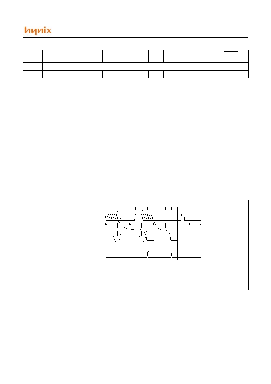
14.1 Power-On Reset (POR)
The GMS77C100X family incorporates on-chip Power-
On Reset (POR) circuitry which provides an internal chip
reset for most power-up situations. To use this feature, the
user merely ties the RESET/V
PP
pin to VDD. A simplified
block diagram of the on-chip Power-On Reset circuit is
shown in Figure 14-1.
The Power-On Reset circuit and the Internal Reset Timer
circuit are closely related. On power-up, the reset latch is
set and the IRT is reset. The IRT timer begins counting
once it detects RESET to be high. After the time-out peri-
od, which is typically 7 ms (oscillation stabilization time),
it will reset the reset latch and thus end the on-chip reset
signal.
FIGURE 14-1 SIMPLIFIED BLOCK DIAGRAM OF ON-CHIP RESET CIRCUIT
V
DD
Internal RESET
WDT Time-Overflow
WDT
Power-On
RESET
Power-Fail
Detect
RESET/V
PP
pin
On-Chip
RC OSC
reset
Internal RESET
Timer ( 8-bit asyn.
ripple counter )
clear
S
R
Q
Q
Noise
Filter
FIGURE 14-2 TIME-OUT SEQUENCE ON POWER-UP (RESET NOT TIED TO V
DD
)
V
DD
RESET
INTERNAL POR
IRT TIMER-OUT
INTERNAL RESET
T
IRT
GMS77C1000/GMS77C1001
34
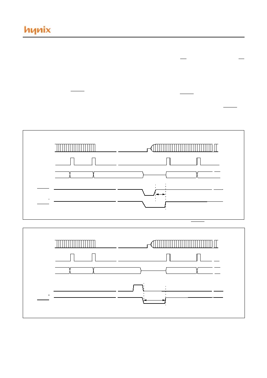
July. 2001 Ver. 1.1
A power-up example where RESET is not tied to VDD is
shown in Figure 14-2. VDD is allowed to rise and stabilize
before bringing RESET high. The chip will actually come
out of reset TIRT after RESET goes high and POR, PFDR
is released.
In Figure 14-3, the on-chip Power-On Reset feature is be-
ing used (RESET and VDD are tied together). The VDD is
stable before the internal reset timer times out and there is
no problem in getting a proper reset. However, Figure 14-
4 depicts a problem situation where VDD rises too slowly.
The time between when the IRT senses a high on the RE-
SET/V
PP
pin, and when the RESET/V
PP
pin (and VDD)
actually reach their full value, is too long. In this situation,
when the internal reset timer times out, VDD has not
reached the VDD (min) value and the chip is, therefore, not
guaranteed to function correctly. For such situations, we
recommend that external R circuits be used to achieve
longer POR delay times (Figure 14-5).
Note: When the device starts normal operation (exits the
reset condition), device operating parameters (volt-
age, frequency, temperature, etc.) must be meet to
ensure operation. If these conditions are not met,
the device must be held in reset until the operating
conditions are met.
FIGURE 14-3 TIME-OUT SEQUENCE ON POWER-UP (RESET TIOED TO V
DD
): FAST V
DD
RISE TIME
FIGURE 14-4 TIME-OUT SEQUENCE ON POWER-UP (RESET TIOED TO V
DD
): SLOW V
DD
RISE TIME
V
DD
RESET
INTERNAL POR
IRT TIMER-OUT
INTERNAL RESET
T
IRT
V
DD
RESET
INTERNAL POR
IRT TIMER-OUT
INTERNAL RESET
T
IRT
- When V
DD
rise slowly, the T
IRT
time-out expires long before V
DD
has reached its final value.
In this example, the chip will reset properly if, V1
V
DD
min.
GMS77C1000/GMS77C1001
July. 2001 Ver. 1.1
35
The POR circuit does not produce an internal reset when
V
DD
declines.
14.2 Internal Reset Timer (IRT)
The Internal Reset Timer (IRT) provides a fixed 7 ms nom-
inal time-out on reset. The IRT operates on an internal RC
oscillator. The processor is kept in RESET as long as the
IRT is active. The IRT delay allows VDD to rise above
VDD min., and for the oscillator to stabilize.
Oscillator circuits based on crystals or ceramic resonators
require a certain time after power-up to establish a stable
oscillation. The on-chip IRT keeps the device in a RESET
condition for approximately 7 ms after the voltage on the
RESET/V
PP
pin has reached a logic high (V
IH
) level and
POR released. Thus, external RC networks connected to
the RESET input are not required in most cases, allowing
for savings in cost-sensitive and/or space restricted appli-
cations. The Device Reset time delay will vary from chip
to chip due to V
DD
, temperature, and process variation.
The IRT will also be triggered upon a Watchdog Timer
time-out. This is particularly important for applications us-
ing the WDT to wake the GMS77C100X from SLEEP
mode automatically.
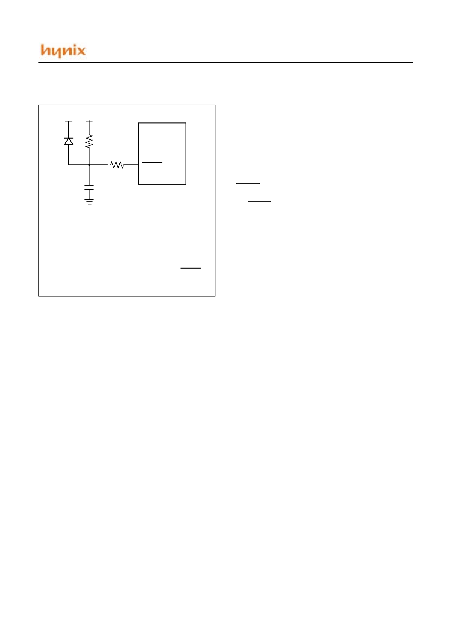
FIGURE 14-5 EXTERNAL POWER-ON RESET
CIRCUIT (FOR SLOW VDD POWER- UP)
RESET
- External Power-On Reset circuit is required only if VDD
power-up is too slow. The diode D helps discharge the
capacitor quickly when VDD powers down.
- R < 40 k
is recommended to make sure that voltage
drop across R does not violate the device electrical specifi-
cation
.
- R1 = 100W to 1 kW will limit any current flowing into
RESET from external capacitor C in the event of RESET
pin breakdown due to Electrostatic Discharge (ESD) or
Electrical Overstress (EOS).
R
R1
D
C
V
DD
V
DD
GMS77C1000/GMS77C1001
36
July. 2001 Ver. 1.1
15. WATCHDOG TIMER (WDT)
The Watchdog Timer (WDT) is a free running on-chip RC
oscillator which does not require any external components.
This RC oscillator is separate from the RC oscillator of the
X
IN
pin. That means that the WDT will run even if the
clock on the X
IN
and X
OUT
pins have been stopped, for ex-
ample, by execution of a SLEEP instruction. During nor-
mal operation or SLEEP, a WDT reset or wake-up reset
generates a device RESET.
The TO bit (STATUS<4>) will be cleared upon a Watch-
dog Timer reset.
The WDT can be permanently disabled by programming
the configuration bit WDTE as a '0' (Figure 12-2). Refer to
the GMS77C100X Programming Specifications to deter-
mine how to access the configuration word.
15.1 WDT Period
The WDT has a nominal time-out period of 14 ms, (with
no prescaler). If a longer time-out period is desired, a pres-
caler with a division ratio of up to 1:256 can be assigned to
the WDT (under software control) by writing to the OP-
TION register. Thus, time-out a period of a nominal 3.5
seconds can be realized. These periods vary with tempera-
ture, V
DD
and part-to-part process variations (see DC
specs).
Under worst case conditions (V
DD
= Min., Temperature =
Max., max. WDT prescaler), it may take several seconds
before a WDT time-out occurs.
15.2 WDT Programming Considerations
The CLRWDT instruction clears the WDT and the
postscaler, if assigned to the WDT, and prevents it from
timing out and generating a device RESET.
The SLEEP instruction resets the WDT and the postscaler,
if assigned to the WDT. This gives the maximum SLEEP
time before a WDT wake-up reset.
FIGURE 15-1 WATCHDOG TIMER BLOCK DIAGRAM
Name
Address
Bit7
Bit6
Bit5
Bit4
Bit3
Bit2
Bit1
Bit0
Power-On
Reset
RESET and
WDT Reset
OPTION
N/A
LOWOPT
PFDEN
T0CS
T0SE
PSA
PS2
PS1
PS0
0011 1111
0011 1111
TABLE 15-1 SUMMARY OF REGISTERS ASSOCIATED WITH THE WATCHDOG TIMER
Postscaler
8
1
0
PSA
MUX
8 - to - 1 MUX
8-bit asynchronous
ripple counter
MUX
PS2:PS0
PSA
1
0
WDT Time-Out
To TMR0
From TMR0 Clock Source
clear
on-chip
RC-OSC
Watchdog Timer
enable
WDTE
SLEEP
clearing WDT
SLEEP
clearing WDT
PSA
GMS77C1000/GMS77C1001
July. 2001 Ver. 1.1
37
16. Power-Down Mode (SLEEP)
For applications where power consumption is a critical
factor, device provides power down mode with Watchdog
operation. Executing of SLEEP Instruction is entrance to
SLEEP mode. In the SLEEP mode, oscillator is turn off
and system clock is disable and all functions is stop, but all
registers and RAM data is held. The wake-up sources from
SLEEP mode are external RESET pin reset and watchdog
time-overflow reset.
16.1 SLEEP
The Power-Down mode is entered by executing a SLEEP
instruction. If enabled, the Watchdog Timer will be cleared
but keeps running, the TO bit (STATUS<4>) is set, the PD
bit (STATUS<3>) is cleared and the oscillator driver is
turned off. The I/O ports maintain the status they had be-
fore the SLEEP instruction was executed (driving high,
driving low, or hi-impedance).
It should be noted that a RESET generated by a WDT time-
out does not drive the RESET pin low.
For lowest current consumption while powered down, the
EC0 input should be at V
DD
or V
SS
and the RESET pin
must be at a logic high level
.
FIGURE 16-1 TIMING DIAGRAM OF WAKE-UP FROM SLEEP MODE DUE TO EXTERNAL RESET PIN RESET
FIGURE 16-2 TIMING DIAGRAM OF WAKE-UP FROM SLEEP MODE DUE TO WATCHDOG TIME-OVERFLOW RESET
~~
Oscillator
(X
IN
pin)
~~
~~
~~
~~
Internal
System Clock
~~
Internal
~~
~~
~~
RESET
RESET
Fetch SLEEP
Execute SLEEP
Fetch RESET vector
~~
~~
Instruction
T
IRT
~~
Oscillator
(X
IN
pin)
~~
~~
~~
~~
Internal
System Clock
~~
Internal
~~
~~
~~
RESET
WDT
Fetch SLEEP
Execute SLEEP
Fetch RESET vector
~~
~~
Instruction
T
IRT
Overflow
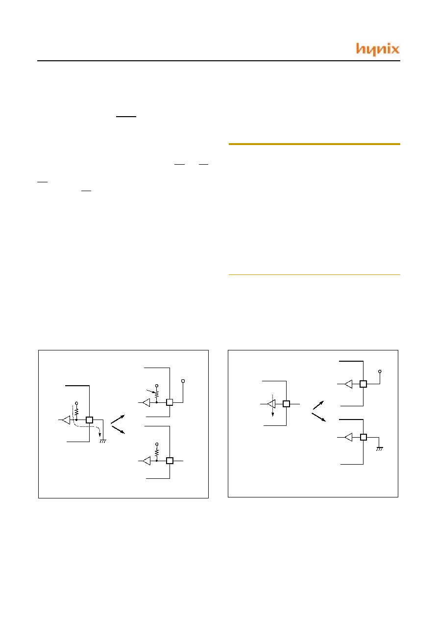
GMS77C1000/GMS77C1001
38
July. 2001 Ver. 1.1
16.2 Wake-up From SLEEP
The device can wake up from SLEEP through one of the
following events:
1.
An external reset input on RESET
pin.
2. A Watchdog Timer time-out reset (if WDT was en-
abled).
3. PFD reset
Both of these events cause a device reset. The TO and PD
bits can be used to determine the cause of device reset. The
TO bit is cleared if a WDT time-out occurred (and caused
wake-up). The PD bit, which is set on power-up, is cleared
when SLEEP is invoked.
The WDT is cleared when the device wakes from sleep, re-
gardless of the wake-up source.
16.3 Minimizing Current Consumption
The SLEEP mode is designed to reduce power consump-
tion. To minimize current drawn during SLEEP mode, the
user should turn-off output drivers that are sourcing or
sinking current, if it is practical.
It should be set properly that current flow through port
doesn't exist.
First conseider the setting to input mode. Be sure that there
is no current flow after considering its relationship with
external circuit. In input mode, the pin impedance viewing
from external MCU is very high that the current doesn't
flow.
But input voltage level should be V
SS
or V
DD
. Be careful
that if unspecified voltage, i.e. if uncertain voltage level
(not V
SS
or V
DD
) is applied to input pin, there can be little
current (max. 1mA at around 2V) flow.
Note: In the
SLEEP
operation, the power dissipation asso-
ciated with the oscillator and the internal hardware
is lowered; however, the power dissipation associat-
ed with the pin interface (depending on the external
circuitry and program) is not directly determined by
the hardware operation of the
SLEEP
feature. This
point should be little current flows when the input
level is stable at the power voltage level (V
DD
/V
SS
);
however, when the input level becomes higher than
the power voltage level (by approximately 0.3V), a
current begins to flow. Therefore, if cutting off the
output transistor at an I/O port puts the pin signal
into the high-impedance state, a current flow across
the ports input transistor, requiring it to fix the level
by pull-up or other means.
If it is not appropriate to set as an input mode, then set to
output mode considering there is no current flow. Setting
to High or Low is decided considering its relationship with
external circuit. For example, if there is external pull-up re-
sistor then it is set to output mode, i.e. to high, and if there
is external pull-down register, it is set to low.
FIGURE 16-3 APPLICATION EXAMPLE OF UNUSED INPUT PORT
INPUT PIN
V
DD
GND
i
V
DD
X
Weak pull-up current flows
V
DD
internal
pull-up
INPUT PIN
i
V
DD
X
Very weak current flows
V
DD
O
O
OPEN
OPEN
i=0
O
i=0
O
GND
When port is configure as an input, input level should
be closed to 0V or 5V to avoid power consumption.
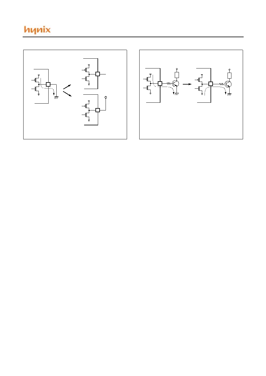
GMS77C1000/GMS77C1001
July. 2001 Ver. 1.1
39
FIGURE 16-4 APPLICATION EXAMPLE OF UNUSED OUTPUT PORT
OUTPUT PIN
GND
i
In the left case, much current flows from port to GND.
X
ON
OFF
OUTPUT PIN
GND
i
In the left case, Tr. base current flows from port to GND.
i=0
X
OFF
ON
V
DD
L
ON
OFF
OPEN
GND
V
DD
L
ON
OFF
To avoid power consumption, there should be low output
ON
OFF
O
O
V
DD
O
to the port.
GMS77C1000/GMS77C1001
40
July. 2001 Ver. 1.1
17. TIME-OUT SEQUENCE AND POWER DOWN STATUS BITS (TO/PD)
The TO and PD bits in the STATUS register can be tested
to determine if a RESET condition has been caused by a
power-up condition, a RESET or Watchdog Timer (WDT)
reset, or a RESET or WDT wake-up reset.
These STATUS bits are only affected by events listed in
Table 17-2.
Note: A WDT time-out will occur regardless of the status of
the TO bit. A SLEEP
instruction will be executed,
regardless of the status of the PD bit.
Table 14-1 lists the reset conditions for the special function
registers, while Table 14-2 lists the reset conditions for all
the registers.
TO
PD
RESET was caused by
1
1
Power-up(POR)
u
u
RESET or PFD reset (normal operation)
1
1. The TO and PD bits maintain their status (
u
) until a reset
occurs. A low-pulse on the RESET input does not change the
TO and PD status bits.
1
0
RESET Wake-up or PFD reset
(from SLEEP)
0
1
WDT reset (normal operation)
0
0
WDT wake-up reset (from SLEEP)
TABLE 17-1 TO/PD STATUS AFTER RESET
Event
TO
PD
Remarks
Power-up
1
1
WDT Time-out
0
u
No effect on PD
SLEEP instruction
1
0
CLRWDT instruction
1
1
TABLE 17-2 EVENTS AFFECTING TO/PD STATUS
BITS
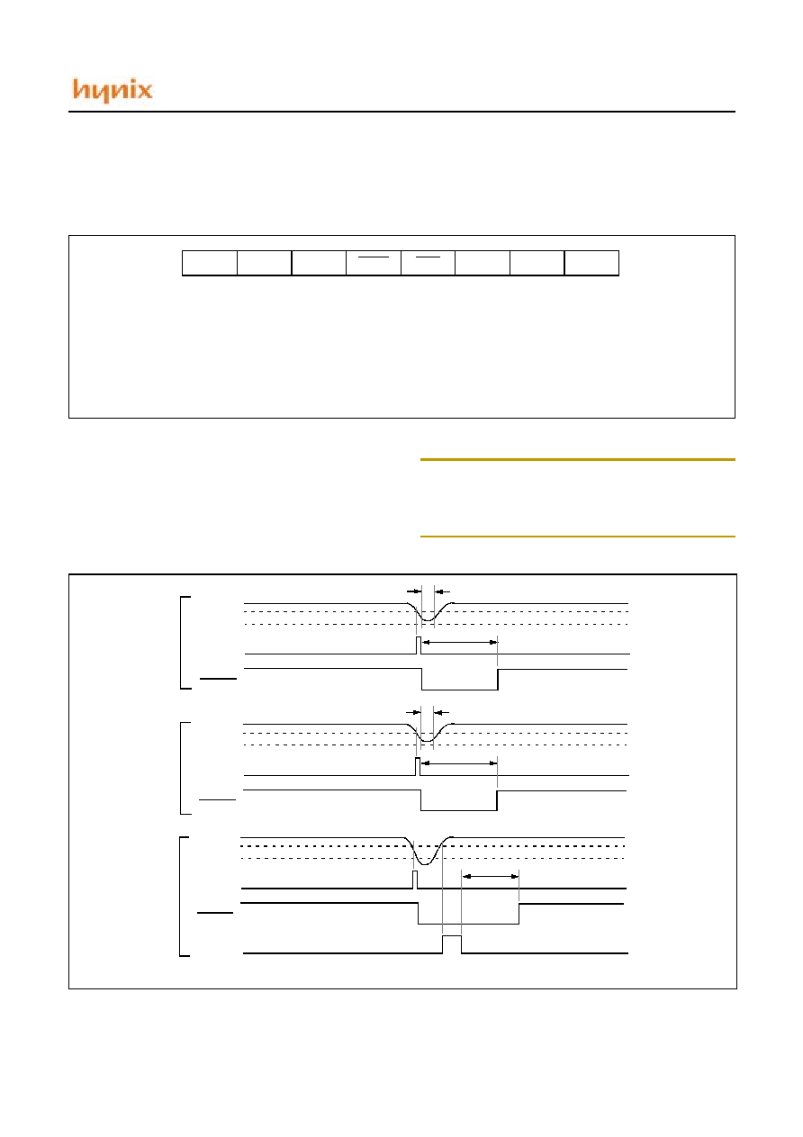
GMS77C1000/GMS77C1001
July. 2001 Ver. 1.1
41
18. POWER FAIL DETECTION PROCESSOR
GMS77C1000X has an on-chip power fail detection cir-
cuitry to immunize against power noise.
If V
DD
falls below a level for longer 100ns, the power fail
detection processor may reset MCU and preserve the de-
vice from the malfunction due to Power Noise.
The bit6(PFDEN) of OPTION register activates the PFD
Circuit, and bit7(LOWopt) lowers the detection level of
the Power Noise. The normal detection level is typically
3V and the lowered detection level is typically 2.5V. Fig-
ure 18-2 shows a Power Fail Detection Situations where
the detection level is selected by LOWOPT Bit.
Note: The PFD circuit is not implemented on the in circuit
emulator, user can not experiment with it. There
fore, after final development user program, this
function may be experimented on OTP
FIGURE 18-1 POWER FAIL DETECTION PROCESSOR
LOWOPT PFDEN
T0CS
T0SE
PSA
PS2
PS1
PS0
bit7
6
bit0
5
4
3
2
1
bit 7
LOWOPT: Power-fail detection level select bit.
1 = Lowered detection level (typ. 2.5V @ 5V)
0 = Normal detection level (typ. 3V @ 5V)
bit 6
PFDEN: Power-fail detection enable bit
1 = Enable power-fail detection
0 = Disable power-fail detection
OPTION
Register
FIGURE 18-2 POWER FAIL DETECTION SITUATIONS
Internal
RESET
V
DD
V
DD
=3V
V
DR
T
NVDD
100nS
PFDEN = 1
PFDR
T
IRT
Internal
RESET
V
DD
V
DD
=2.5V
V
DR
T
NVDD
100nS
PFDR
T
IRT
Internal
RESET
V
DD
V
DD
=3/(2.5)V
V
DR
PFDR
T
IRT
POR
LOWOPT = 0
PFDEN = 1
LOWOPT = 0/1
V
DD
V
DR
PFDEN = 1
LOWOPT = 1
When VDD falls below approximately 1V level, Power-On Reset may occur.
Document Outline